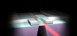
Quantum Nano-Electronics & Nano-Photonics
Domestic Conference Papers(78 including 44 first author papers and 31 invited talks.)
1.1.S. Saito, “Novel Transport Properties in Quantum Confined Silicon Channels”, The third scientific forum, Nanotechnology: Advances and Research, Saudi Arabian Cultural Bureau in London (Southampton, 2018) [invited].
2.S. Saito, “Introduction to Nanoelectronics for Quantum Technologies”, Quantum, Light & Matter Summer School, (Winchester, 2016) [invited].
3.S. Saito, “Development of germanium light sources monolithically integrated on silicon”, SG-UK Photonics Coloquium, (Southampton, 2016) [invited].
4.S. Kako, S. Ishida, K. Oda, S. Saito, T. Ido, and Y. Arakawa, “Fabrication and optical characterization of microdisk cavities using directly grown Ge on SOI”, The 62th Japan Society of Applied Physics Spring meeting (Tokai University, 2015).
5.A. Z. Al-Attili, M. Husain, F. Gardes, and S. Saito, “Group IV Photonics: Ge Light Emission”, Nano Group Workshop (University of Southampton, 2014) [Best Poster Award].
6.S. Saito, “End of Scaling? Challenges & Opportunities in Device Physics”, IEEE Student Union (University of Southampton, 2013) [invited].
7.Y. Suwa and S. Saito, “First-Principles Study of Optical Grain in Strained Germanium”, OPE, IEICE (2012).
8.K. Tani, S. Saito, K. Oda, T. Okumura, T. Mine, and T. Ido, “Development of Ge Light Emitter for Monolithic Light Sources”, LQE, IEICE (2012).
9.M. Sagawa, Y. Lee, Y. Suwa, and S. Saito, “Laser oscillation conditions in Si/Ge quantum wells”, The 72th fall meeting of Japan Society of Applied Physics (2011).
10.S. Saito , "Silicon Quantum Well Light-Emitting Diode Fabricated by Micorofabrication Techniques", The
Institute of Electronics, Information, and Communication Engineers (IEICE), CI-3-4, (Tokyo, 2011) [invited].
11.S. Saito , "Silicon Quantum Well Light-Emitting Diode", The Institute of Electronics of Japan, (Waseda, 2011) [invited].
12.D. Hisamoto, S. Saito, A. Shima, H. Yoshimoto, K. Torii, and E. Takeda, “A New Approach for Steep Subthreshold Swing (SS) FET”, SDM, IEICE 110, pp. 39-42 (2011).
13.T. Sugawara, Y. Matsuoka, S. Saito, N. Matsushima, and S. Tsuji, “Research Trends and Future Directions for Optical Interconnects Technologies”, Design Gaia (2010) [invited].
14.Y. Suwa and S. Saito, “First principle calculation on silicon quantum well light emitter”, Gakushin 145 committee (2010) [invited].
15.S. Saito and Y. Suwa, “Silicon quantum well light-emitting device”, the 13th quantum nanoelectronics seminar (2010) [invited].
16.S. Saito, “Optical interconnection by silicon light-emitter”, Gakushin 154 committee (2010) [invited].
17.S. Saito, “Ultra-thin Silicon light source”, OITDA (2010) [invited].
18.Y. Nagami, Y. Tsuchiya, S. Saito, T. Arai, H. Shimada, H. Mizuta, K. Uchida, and S. Oda, “NEMS memory characteristics and scaling under trap-assisted tunneling in pn-junction”, The 56th Japan Society of Applied Physics (2009).
19.Y. Suwa and S. Saito, “Enhanced light emission from ultra-thin silicon by strain”, the 2009 fall meeting of physical society of Japan (2009).
20.Y. Suwa and S. Saito, “Electroluminescence mechanism from ultra-thin silicon by first principle calculations”, the 64th physical society of Japan meeting (2009).
21.H. Uchiyama, T. Kawamura, H. Wakana, and S. Saito, “Fully depleted TFT of amorphous oxide”, Gakushin 151 committee (2009).
22.S. Saito and H. Uchiyama, “Application of neo-silicon”, The 70th Japan Society of Applied Physics (Toyama, 2009).
23.S. Saito, “Silicon light-emitting device”, Optronics special technology seminar on green photonics (2009) [invited].
24.S. Saito, “Optical gain in ultra-thin silicon light-emitting diode”, the 39th OPT research workshop (2009) [invited].
25.M. Muraguchi, T. Endo, Y. Sakurai, S. Nomura, H. Takada, K. Shiraishi, M. Ikeda, K. Makihara, S. Miyazaki, and S. Saito “Electron Dynamics in Electron Gas Coupled with Quantum Dots II”, the Physical Society of Japan (2009).
26.S. Saito, “Ultra-thin silicon light-emitting diode”, JEITA silicon photonics committee (2008) [invited].
27.M. Muraguchi, H. Takada, S. Nomura, Y. Sakurai, S. Saito, and K. Shiraishi, “Electron dynamics in electron gas – quantum dot coupling system”, the Physical Society of Japan (2008).
28.Y. Nagami, S. Matsuda, Y. Tsuchiya, S. Saito, T. Arai, H. Shimada, H. Mizuta, and S. Oda, “Transient response characteristics in NEMS memory device with damping”, The 55th Japan Society of Applied Physics (2008).
29.S. Saito, “Electroluminescence from ultra-thin silicon”, optoronics seminer (Chuo university, 2007) [invited].
30.S. Saito, “Electroluminescence from ultra-thin silicon”, silicon photonics workshop (Tokyo institute of technology, 2007) [invited].
31.S. Saito, “Electroluminescence from ultra-thin silicon”, the 10th polymer optical circuit research community (Keio university, 2007) [invited].
32.S. Saito, “Electroluminescence from ultra-thin silicon”, OITDA meeting (Tokyo, 2007) [invited].
33.S. Saito, “Silicon light-emitting transistor”, The 68th Japan Society of Applied Physics (Hokkaido, 2007) [invited].
34.S. Saito, “Ultra-thin silicon light-emitting transistor for on-chip optical interconnection”, JEITA nanoelectronics technology committee (2007) [invited].
35.S. Saito, D. Hisamoto, H. Shimizu, H. Hamamura, R. Tsuchiya, Y. Matsui, T. Mine, T. Arai, N. Sugii, K. Torii, S. Kimura, and T. Onai, “Electroluminescence from ultra-thin single crystalline silicon”, Gakushin 125 committee (Tsukuba university, 2007) [invited].
36.S. Saito, D. Hisamoto, H. Shimizu, H. Hamamura, R. Tsuchiya, Y. Matsui, T. Mine, T. Arai, N. Sugii, K. Torii, S. Kimura, and T. Onai, “Electroluminescence from ultra-thin silicon”, Gakushin 151 committee (Atami, 2007) [invited].
37.S. Saito, “Silicon light-emitting transistor for realization of on-chip optical interconnection”, Silicon photonics research community (The university of Tokyo, 2007) [invited].
38.S. Saito, D. Hisamoto, Y. Kimura, N. Sugii, R. Tsuchiya, K. Torii, and S. Kimura, “Drive current enhancement mechanism in <100> channel pMOSFET”, the Japan Society of Applied Physics, silicon technology division (Atagawa, 2007) [invited].
39.S. Saito, “Electroluminescence from ultra-thin silicon”, the Japan Society of Applied Physics, quantum electronics division (Karuizawa, 2007) [invited].
40.A. Tanaka, Y. Tsuchiya, K. Usami, S. Saito, T. Arai, H. Mizuta, and S. Oda, “Fabrication of LB film of silicon nano-crystalline dots with surface passivation”, The 68th Japan Society of Applied Physics (2007).
41.J. Shibata, B. Pruvost, Y. Tsuchiya, K. Usami, S. Saito, H. Mizuta, and S. Oda, “Observation of pull-in operation in suspended gate MOSFET by C-V measurements”, The 68th Japan Society of Applied Physics (2007).
42.S. Matsuda, Y. Nagami, Y. Tsuchiya, S. Saito, T. Arai, H. Shimada, H. Mizuta, and S. Oda, “KFM observation of charge injected 2-dimentional silicon nano-dot layer for realization of NEMS memory device”, The 68th Japan Society of Applied Physics (2007).
43.S. Saito, D. Hisamoto, Y. Kimura, N. Sugii, R. Tsuchiya, K. Torii, and S. Kimura, “Drive current enhancement mechanism in <100> channel pMOSFET”, the Japan Society of Applied Physics, silicon technology division for VLSI technology reports (The University of Tokyo, 2006) [invited].
44.T. Arai, S. Saito, H. Fukuda, and K. Torii, “Chemical control of 2D artificial lattice of gold nano-particles”, The 53th Japan Society of Applied Physics (Musashi institute of technology, 2006).
45.Y. Nagami, S. Momo, Y. Tsuchiya, S. Saito, T. Arai, H. Shimada, H. Mizuta, and S. Oda, “Operation voltage reduction for NEMS memory devices by 3-dimentional finite element simulation”, The 53rd Japan Society of Applied Physics (2006).
46.Y. Nagami, S. Matsuda, Y. Tsuchiya, S. Saito, T. Arai, H. Shimada, H. Mizuta, and S. Oda, “Analysis on read-out characteristics in NEMS memory devices by finite element simulation”, The 67th Japan Society of Applied Physics (2006).
47.S. Matsuda, Y. Nagami, Y. Tsuchiya, S. Saito, T. Arai, H. Shimada, H. Mizuta, and S. Oda, “Switching operation under the application of voltage in NEMS memory”, The 67th Japan Society of Applied Physics (2006).
48.H. Mizuta, Y. Nagami, B. Pruvost, S. Momo, J. Ogi, S. Matsuda, J. Shibamura, Y. Tsuchiya, S. Saito, T. Arai, Y. Kimura, H. Shimada, and S. Oda, “Functional silicon nano-devices with nano-electro-mechanical structures”, the 85th silicon technology committee, The Japan Society of Applied Physics (2006).
49.S. Momo, Y. Nagami, Y. Tsuchiya, S. Saito, T. Arai, H. Shimada, H. Mizuta, and S. Oda, “Fabrication of double bridge structure for realization of NEMS memory devices”, The 53rd Japan Society of Applied Physics (2006).
50.S. Saito, “Mobility reduction mechanisms in MISFET with high-k gate dielectrics”, the 23th nanostructure system technology community, (Waseda university, 2005) [invited].
51.Y. Nagami, S. Momo, Y. Tsuchiya, S. Saito, T. Arai, H. Shimada, H. Mizuta, and S. Oda, “High precision switching characterization by taking strain on NEMS memory devices”, The 52th Japan Society of Applied Physics (2005).
52.G. Yamahata, A. Tanaka, Y. Kawata, Y. Tsuchiya, S. Saito, T. Arai, H. Mizuta, and S. Oda, “Fabrication of silicon nano dot cluster devices by solution dissolved nano-crystalline silicon dots”, The 52th Japan Society of Applied Physics (2005).
53.Y. Nagami, S. Momo, Y. Tsuchiya, S. Saito, T. Arai, H. Shimada, and H. Mizuta, and S. Oda, “Dynamical switching characteristics of NEMS memory device”, The 65th Japan Society of Applied Physics (2004).
54.S. Saito, “Mobility reduction model by variations of dielectrics”, the Japan Society of Applied Physics, silicon technology division, the 9th meeting on ultra-thin silicon-dioxide formation, characterization, and reliability (Atagawa, 2004) [invited].
55.S. Saito, D. Hisamoto, M. Hiratani, and S. Kimura, “Unified mobility model for high-k gate dielectrics”, the Japan Society of Applied Physics, IEDM reports on advanced CMOS device process technology (Tokyo, 2003) [invited].
56.S. Saito, Y. Matsui, K. Torii, Y. Shimamoto, D. Hisamoto, M. Hiratani, and S. Kimura, “Mobility reduction mechanisms in MISFETs with high dielectric constant gate dielectrics”, applied electron material division, current status and future perspective on high dielectric constant gate dielectrics (Tokyo, 2003) [invited].
57.S. Saito, Y. Matsui, K. Torii, Y. Shimamoto, D. Hisamoto, M. Hiratani, and S. Kimura, “Mobility reduction by phase separation in high-k dielectrics”, The 64h Japan Society of Applied Physics, (2003).
58.S. Saito, “Mobility reduction in MISFETs with high dielectric constant gate dielectrics”, The 64th semiconductor integrated circuits technology symposium (Osaka, 2003) [invited].
59.S. Saito, “Mobility reduction mechanism by remote-charge-scattering in MISFET with Al2O3 high-k gate dielectrics”, the 4th electronic society committee meeting on dielectrics thin film materials fundamentals and characterization technology (2003).
60.M. Hiratani, K. Torii, Y. Shimamoto, S. Saito, and J. Yugami, “Interface engineering on high dielectric oxide/Si”, the institute of electronics, information, and communication engineers, SDM workshop (Tohoku university, 2002).
61.K. Torii, Y. Shimamoto, S. Saito, O. Tonomura, M. Hiratani, and Y. Manabe, M. Caymax, J. W. Maes, “Mobility reduction in MISFET with Al2O3 gate dielectrics”, Silicon nanotechnology division, ULSI research workshop (2002).
62.Y. Shimamoto, O. Tonomura, S. Saito, K. Torii, and M. Hiratani, “Evaluation of Mobility in the MOSFET with Large Leakage Current” SDM, IEICE 102, pp. 39-44 (2002).
63.K. Torii, Y. Shimamoto, S. Saito, T. Yamauchi, M. Hiratani, and T. Onai, “Mobility reduction by fixed charges in Al2O3 gate dielectrics FET” , The 49th Japan Society of Applied Physics (2002).
64.K. Torii, S. Saito, T. Yamauchi, and M. Hiratani, “Zirconium silicate characteristics dependence on zirconium contents ” , The 49th Japan Society of Applied Physics, p. 830 (2002).
65.K. Torii, Y. Shimamoto, S. Saito, T. Yamauchi, M. Hiratani, and T. Onai, “Mobility improvement by interface engineering on Al2O3 gated MISFET”, the Japan Society of Applied Physics, silicon technology division, the 8th meeting on ultra-thin silicon-dioxide formation, characterization, and reliability (Atagawa, 2002).
66.S. Saito, Y. Shimamoto, S. Tsujikawa, O. Tonomura, T. Mine, R. Tsuchiya, K. Ohnishi, H. Hamamura, J. Yugami, K. Torii, D. Hisamoto, M. Hiratani, T. Onai, and S. Kimura, “Coulomb scattering in MISFET with ultra-thin silicon oxynitride”, The 50th Japan Society of Applied Physics, p. 810 (2002).
67.S. Saito, Y. Shimamoto, O. Tonomura, K. Torii, Y. Manabe, M. Caymax, J. W. Maes, M. Hiratani, T. Onai, and S. Kimura, “Mechanism of mobility reduction in MISFETs with Al2O3/SiO2 gate stacks”, The 63th semiconductor integrated circuits technology symposium (2002) [Symposium Award].
68.S. Saito, Y. Shimamoto, O. Tonomura, K. Torii, Y. Manabe, M. Caymax, J. W. Maes, M. Hiratani, T. Onai, and S. Kimura, “Mechanism of mobility reduction in MISFETs with Al2O3/SiO2 gate stacks”, The 63th Japan Society of Applied Physics, p. 747 (2002).
69.S. Saito, Y. Shimamoto, O. Tonomura, K. Torii, M. Hiratani, T. Onai, and S. Kimura, “Quantum mechanical analytical models on chapacitance-voltage characteristics” The 63th Japan Society of Applied Physics, p. 718 (2002).
70.S. Saito, Y. Shimamoto, K. Torii, M. Hiratani, T. Onai, and S. Kimura, “Quantum mechanical analysis on ultra-thin gate dielectric MOSFET”, Japan Society of Applied Physics silicon technology division workshop on gate dielectrics in 100nm technology node, (Hiroshima, 2002).
71.S. Saito, K. Torii, M. Hiratani, and T. Onai, “Analytic model of quantum effects on MOS accumulate capacitance” The 49th Japan Society of Applied Physics, p. 810 (2002).
72.S. Saito, K. Torii, M. Hiratani, and T. Onai, “Quantitative theory of remote charge scatterings” The 49th Japan Society of Applied Physics, p. 817 (2002).
73.K. Torii, Y. Shimamoto, S. Saito, M. Hiratani, T. Onai, and T. Yamauchi, “Mobility reduction mechanism by variations of dielectric constant”, the Japan Society of Applied Physics, silicon technology division, the 7th meeting on ultra-thin silicon-dioxide formation, characterization, and reliability (Atagawa, 2001).
74.S. Saito, H. Yoshimoto, Y. Y. Suzuki, S. Kurihara, “Quantum phase transition in the infinite dimensional Hubbard model”, fundamental physics research laboratory short period workshop on new frontier of magnetic phenomena by quantum effects (1998).
75.S. Saito, Y. Y. Suzuki, S. Kurihara, “Ground state in infinite dimensional attractive Hubbard model”, The 54th annual meeting of physical society of Japan (1999).
76.S. Saito, Y. Y. Suzuki, S. Kurihara, “Superconducting phase transition in infinite dimensional Hubbard model”, The 53th annual meeting of physical society of Japan (1998).
77.S. Saito, S. Kurihara, “Quantum phase transition from Fermi liquid to antiferromagnets”, The fall meeting of physical society of Japan (1997).
78.S. Saito, S. Kurihara, “Coexistence of superconductivity and charge-density-waves in the attractive Hubbard model”, The 52th annual meeting of physical society of Japan (1997).