Quantum Nano-Electronics & Nano-Photonics
Thousands of Multiple-Quantum-Wells on Si...
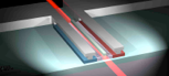
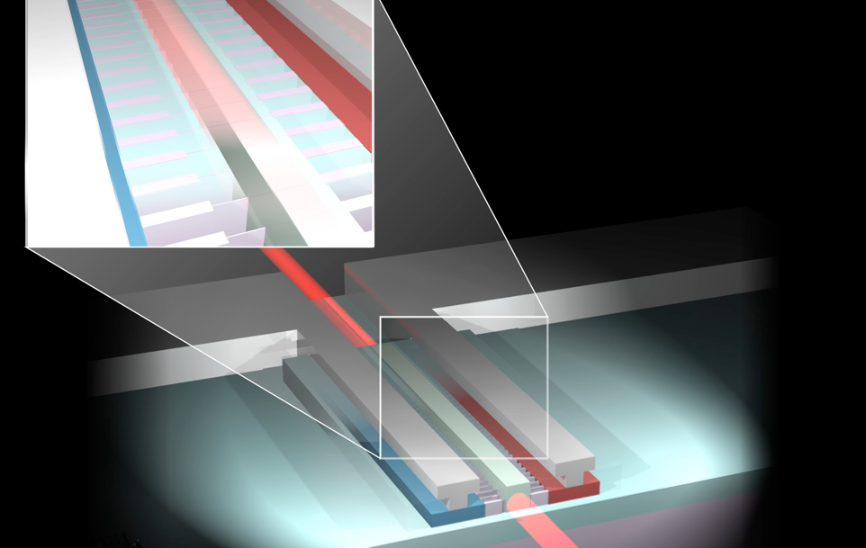
Conventional wisdom to enhance the light-emission capabilities is to increase the number of quantum wells: from Single-Quantum-Well (SQW) to Multiple-Quantum-Wells (MQWs). In III-V compounds, the extension was straightforward, since MQWs were developed by the epitaxial growth technologies. On the other hand, Si is based on the planar technologies and it is difficult to prepare the vertical stacks of crystalline films. Then, we considered to prepare the vertical MQWs periodically aligned on the Si substrate. The structure is called as a “fin”. Si Fin was invented my senior colleague of Dr. D. Hisamoto (Hitachi), and recently fin based field-effect-transistors have been integrated in our MPUs. With his advise on fabrications, I have made a Si fin based LED for the first time. Si fins worked as MQWs for light emissions, and the Si3N4 waveguide cavity was fabricated to confine the optical waves with distributed-feedback (DFB) due to the periodic fin structures.
Si fin Light-Emitting Diode
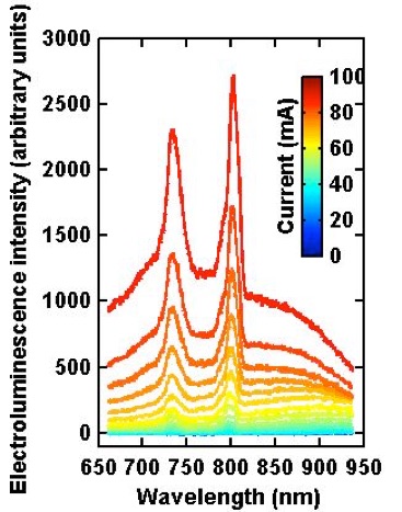
Enhanced emissions observed from the edge...
still we need another idea for lasing...
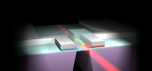
According to our first-principle calculations, we can expect direct recombination in ultra-thin Si Quantum-Well by conduction band valley projections. We have confirmed strong photo-luminescence from Si QW (001) with thickness down to or less than 1.0 nm (5 atomic layers). It was difficult to accommodate the compatibility between quantum confinements and carrier injections. To achieve it, we employed lateral carrier injections suitable for Si processes, and fabricated a Si QW Light-Emitting-Diode (LED) with Si3N4 optical waveguide.
Ge is an another Group-IV material suitable for Si processes, but again, Ge has an indirect band gap.
We are developing further toward the first
Si/Ge fin Laser Diodes.
Ge oxidation condensation of SiGe fins.
Excellent crystalline quality!
Collaborators:
Prof. Y. Arakawa, Prof. S. Iwamoto, Dr. S. Kako (University of Tokyo).
Drs. T. Ido, Y. Suwa, K. Tani, K. Oda, M. Sagawa, J. Kasai, (PETRA, PECST, Hitachi), T. Okumura, M. Takahashi, E. Nomoto, T. Mine, Y. Lee, H. Arimoto,
-
N.Sakuma, D. Hisamoto, H. Uchiyama, J. Yamamoto, T. Sakamizu,
S. Kimura, T. Sugawara, and M. Aoki, and more engineering support staffs (Hitachi).
Germanium is an another material suitable for the monolithic integration to a Si chip. Ge is the same group-IV material as Si and expected to be promising for high speed transistors and photodetectors. However, again, Ge has an indirect band gap. The strategy to use Ge for light-emissions is slightly different from that of Si. The band structure of Ge is more closer to that of direct band gap III-V materials. To enhance the light-emissions from Ge, researchers are trying to dope impurity donors to occupy the indirect conduction band valleys so that electrons are injected at the direct band valley. Another strategy is to apply the tensile stress to Ge to decrease the direct band gap.
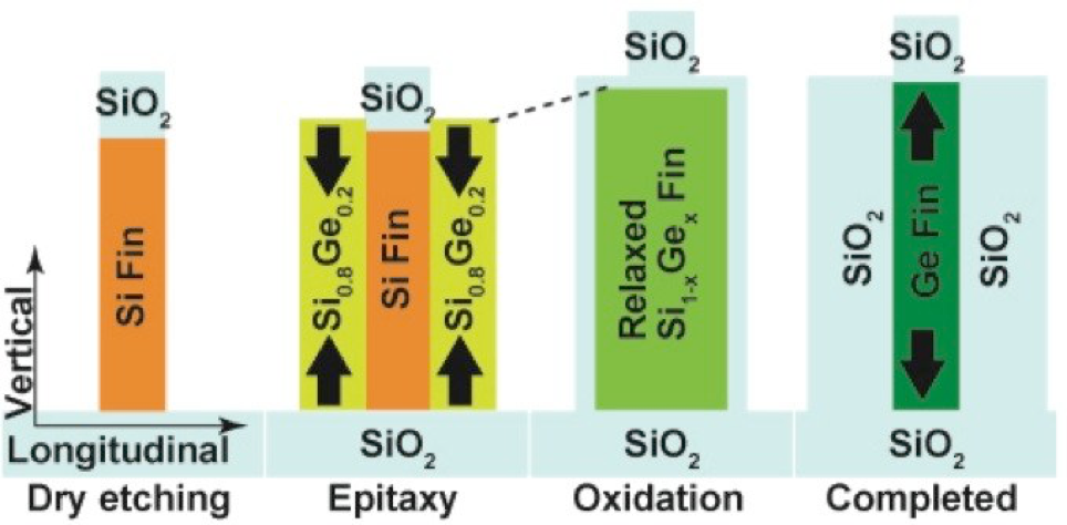
For both strategies, the preparation of Ge with high crystalline quality is critical, otherwise the injected carriers would recombine at the defects without luminescence. However, the lattice constant between Si and Ge is 4.2 %. This huge difference prevents the direct epitaxial growth of Ge on Si without the formation of significant amount of crystalline dislocations. To overcome this issue, we applied the Ge oxidation condensation technique to SiGe fins, in order to relax the strain.
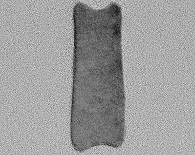


Ge fin
SiO2
SiO2
Si
Si3N4
During the Ge oxidation condensation, Si is selectively oxidized and Ge is dissolved inside SiGe fins due to the difference of the oxide formation energies. At the same time, fins can be stretched out to relax the strain inside the fins. The oxidation time is precisely controlled to form the pure Ge fins.
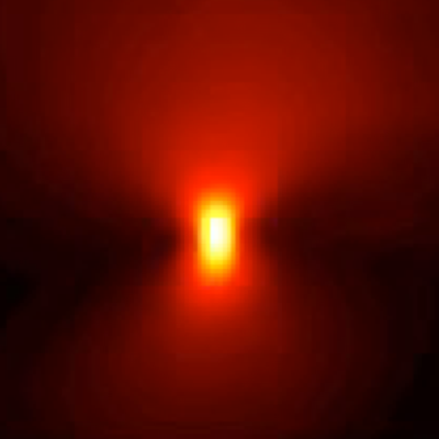
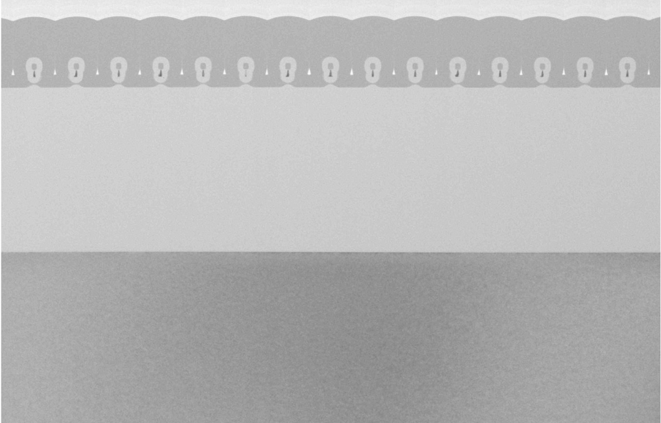
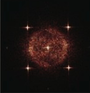
We have confirmed the perfect crystalline structure of Ge fins by transmission-electron-microscope. We also found that the low dark current of the Ge fin diode under the application of the reverse bias. By injecting currents to Ge fins, we observed light emissions at around 1600nm, which will be suitable for various Si photonics optical circuits as well as fibre optics.