CVD processing
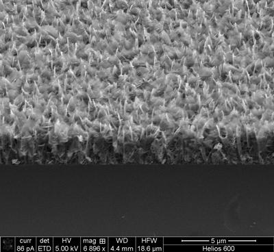
Here at the University’s Optoelectronics Research Centre (ORC), we have developed chemical vapour deposition (CVD) processes to produce large-area thin films and 2D material systems. We are now working on investigating their properties and device functionality based on these materials. Our breadth of expertise and the application areas we are targeting are shown in the table below.
| Compound Synthesized | Applications |
| Ge-S | Optical, electronics, Nano |
| Sb-S | Optical, electronics, Nano |
| Ge-Sb-S | Optical, electronics |
| Ge-Sb-Te (GST) | Electronics |
| Ti-S | Tribology, battery, thermoelectric |
| Sn-S | Transistor |
| Mo-S | Transistor, tribology |
| W-S | Transistor, tribology |
| Cu-In-Ga-S / Se (CIGS) | Solar |
| Cu-Zn-Sn-S (CZTS) | Solar |
| Cu-Sb-S | Solar |
| Ti-O | Transparent conducting oxides, solar |
| Zn-O | Transparent conducting oxides, solar |
| Sn-O | Transparent conducting oxides, solar |
| Hybrid Sb-O/Sb-S | Memristor |
| Hybrid Ge-O/Ge-S | Memristor |
| Graphene | Solar, transistor |
Technological advantages of CVD process for thin films
- Low-cost atmospheric pressure process, scalable to large areas
- Large range of material systems with wide ranging properties can be deposited using process
Technology Roadmap
- 2002 First demonstration (EPSRC funded) of the synthesis of chalcogenides by CVD (patent granted)
- 2004 Commence work on electronic memory applications of GLS (EPSRC funded)
- 2006 First demonstration of electrical phase change switching and memory in GLS thin film (patent granted)
- 2011 First demonstration of phase change switching in CVD deposited thin film
- 2012 Commence programme in 2D chalcogenides thin films through the EPSRC Centre of Innovative Manufacturing in Photonics
- 2013 Commence programme in the use of atomic layer deposition of chalcogenides
Collaboration opportunity
We would be interested in working with partners with application-driven requirements for 2D material systems and thin films.
If you would like to know more please contact Professor Dan Hewak dh@orc.soton.ac.uk or Dr Kevin Huang cch@orc.soton.ac.uk
Related Staff Member

Professor Dan Hewak
Professor Dan Hewak is part of our interdisciplinary research collaborations in Aerospace at the University of Southampton.
View profileLinks to external websites
The University cannot accept responsibility for external websites.