Research project: Reid: Electrodeposition of Semiconducting Chalcogenides from Unusual Media
Currently Active:
Yes
Semiconducting metal chalcogenides are of increasing importance for emerging micro- and nano-electronic applications in renewable energy, solid state memory and 3D metamaterials. However, the demand for smaller, higher performance, more energy-efficient electronics, is pushing conventional materials deposition and device fabrication methods to their intrinsic limits. ‘Top-down’ vapour deposition methods are not suitable for filling very high aspect-ratio vias in structures that may be the basis of future devices. Electrodeposition offers several potentially significant advantages: it is a faster and much lower cost alternative to vapour deposition, and as a ‘bottom-up’ growth method, it can fill 2D and 3D nanostructures selectively. Electrodeposition is therefore an extremely attractive prospect for the production of nano-structured materials and devices.
Project Overview
click on image to expand
(a) Electrodeposition of Device-Quality Phase Change Memory (PCM) Materials
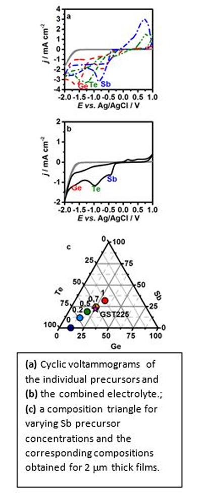
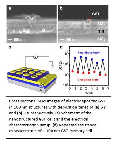
PCM is a non-volatile memory type that works on the principle of probing the resistivity of the memory material, which is either amorphous or crystalline, by means of an electrical pulse. Rewriting of the memory bits is achieved by either re-crystallising an amorphous cell with a medium-amplitude voltage SET pulse or re-amorphising a crystalline cell with a high-amplitude voltage RESET pulse (cycling). Materials required for PCM applications are characterised by their high contrast between the resistances of the crystalline and amorphous phases, very fast phase transition speeds (tens of nanoseconds) and high stabilities. Chalcogenide-based PCM materials are among the most promising candidates to scale non-volatile memory beyond the Flash memory architecture, with the ternary Ge2Sb2Te5 (GST-225) the most widely used. Electrodeposition offers a highly effective alternative approach for the deposition of such materials, offering excellent spatial selectivity. In collaboration with Profs. Bartlett and Hector (Chemistry) and de Groot (ECS) and with funding from EPSRC, we have developed a highly tuneable electrolyte system for the electrodeposition of phase change memory materials, including the challenging ternary GST-225, from CH2Cl2. The system allows fine control of the ternary composition across the whole phase diagram, and rapid, highly efficient deposition into arrays of sub-100 nm nano-cells. Using this approach we have produced functional nano-devices with highly promising phase cycling and endurance lifetimes (Materials Horizons, 2015, 2, 420; doi:10.1039/C5MH00030K; RSC Advances, 3, 15645; doi:10.1039/c3ra40739j).
click on image to expand
(b) Electrodeposition of Extreme Nanostructured Materials from Supercritical Fluids
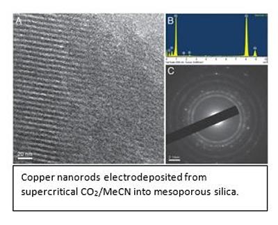
Supercritical fluid electrodeposition (SCFED) is a materials deposition technique that exploits the unique properties of supercritical fluids (SCFs), most notably, their lack of surface tension and their high mass transport rates, to enable electrodeposition of materials into high aspect ratio, extremely narrow diameter pores. As part of the EPSRC Programme Grant, ‘Complex Nanostructures by Supercritical Fluid Electrodeposition’ (www.scfed.net) led by Prof. Phil Bartlett we have shown that it is possible to deposit a range of metal and reactive materials from SCFs, including Ge, Ag and Cu, of which 3 nm nanowires have been grown for the latter (Proc. Natl. Acad. Sci., USA 2009, 106, 14768; doi:10.1073/pnas.0901986106; ChemElectroChem, 2014, 1, 187; doi:10.1002/celc.201300131; Phys. Chem. Chem. Phys. 2014, 16, 9202; doi:10.1039/c3cp54955k; Chemistry - A European Journal, 2014, 20, 5019; doi:10.1002/chem.201400179).
click on image to expand
click on image to expand
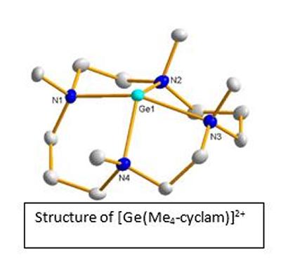
The development of SCFED to enable the formation of a wide range of elements from the main group (Ga, In, Ge, Sn, Pb, Sb, Bi, Se, Te) has been achieved, and sub-13 nm nanowires of several of these demonstrated, including binary and ternary semiconductors for electronic and optical applications. This work has required development of tailored reagents to provide the source of the elements being deposited, and therefore we have developed several series of unusual complexes based upon dicationic Ge aza-macrocyclic species such as [Ge(Me3-tacn)]2+ and [Ge(Me4-cyclam)]2+ (Angew. Chem. Int. Ed. 2009, 48, 5152; doi:10.1002/anie.200901247) and rare soft phosphine complexes of Ge(II) and Si(IV) (Inorg. Chem. 2010, 49, 752; doi:10.1021/ic902068z; Inorg. Chem. 2013, 52, 5185; doi:10.1021/ic400077z)
click on image to expand
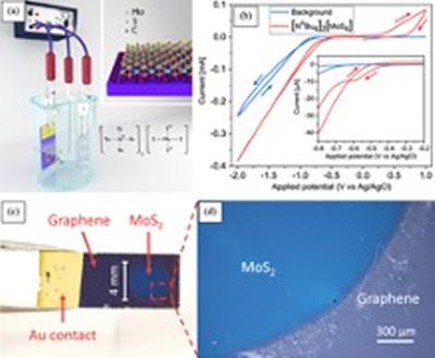
(c) Electrodeposition of few-layer transition metal dichalcogenides from weakly coordinating solvents
Under a current EPSRC project we are developing electrolytes that allow the electrodeposition of transition metal dichalcogenide semiconductors, including MoS2 and WS2 and have recently demonstrated electrodeposition of few-Layer MoS2 on graphene for 2D material heterostructures (ACS Adv. Mater. and Interfaces, 2020, 12, 44, 49786; https://dx.doi.org/10.1021/acsami.0c14777).