If you are reading a paper copy of this document, your first task is to find the corresponding web page so that you can make use of the javascript walkthroughs (just click on one of the little coloured icons at the end of a paragraph).
First change to a suitable directory (in general a new directory should be used whenever a new design is started):
cd ~/design/magic/test
This directory should already exist but if not it can be created using the mkdir command.
To start magic using the On Semi 0.35µm CMOS process type magic -T c035u. A new window will appear. (Magic can also accept a design name on the command line, e.g. magic -T c035u example.)
If magic won't start you may need use the
remote login facility to access one of the older servers
which run a slightly different version of the Linux operating system
(Hart):
Applications -> Remote Login -> Hart
Move the mouse pointer over the new window. Notice that the border of the new window becomes highlighted and the cursor changes from an arrowhead to a crosshair. This is an indication that the active window has changed merely because the mouse has moved (no mouse click is required). Magic expects this focus follows mouse behaviour, if this doesn't happen for you, seek help from a laboratory demonstrator.
Commands to magic are given in three ways: through the mouse,
as single character macros and as long commands starting with
a colon (:). To start editing a cell, magic requires a cell name.
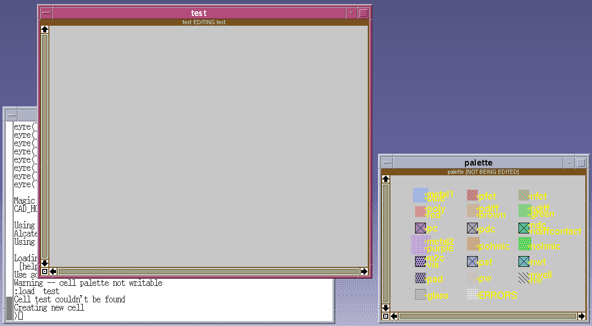
Type :load test. Magic responds with Cell test couldn't
be found. Creating new cell. The frame of the new window
changes to test EDITING test.
![]()
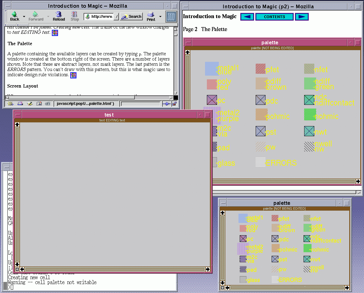
The Palette
A palette containing the available layers can be created by typing
p. The palette window is created at the bottom right
of the screen. There are a number of layers shown. Note that
these are abstract layers, not mask layers. The last pattern
is the ERRORS pattern. You can't draw with this pattern,
but this is what magic uses to indicate design rule violations.
![]()
Screen Layout
Whenever you run magic you should arrange your windows on the screen as shown below:
The main editing window takes up a large part of the screen, overlapping with the terminal window from which magic was started. The bottom few lines of text in the terminal window are clearly visible. Do not be tempted to "maximise" the editing window (so that it occupies the whole screen) since you will not be able to see the information, warning and error messages provided by magic.
Unless you are fortunate enough to have access to a computer with two screens when you run this tutorial, you will have to display two web browser windows on the screen at the same time as the three magic windows.
A suggested layout is shown below with a small browser window top left and the javascript popup window top right:
It's a tight squeeze but the benefits of being able to navigate the javascript walkthrough while you are working on your own design outweigh the disadvantages of having to use smaller windows. Of course none of this will work if your screen resolution is set too low; a resolution of 1280x1024 or greater is ideal.
NMOS Transistor
To show how magic works with abstract layers, we'll start by drawing
an NMOS transistor. Move the crosshair cursor to the left of
and below the centre of the editing window. Click the left
mouse button. A small box appears. Now move the cursor up about
a third of the window and slightly to the right. Click the right
mouse button. The box changes to a long thin rectangle. Now
move the cursor over the red patch labelled poly in the
palette window. Click the middle mouse button. The box in the
editing window is now filled with the poly pattern. This
poly "tile" will provide the gate connection for our first
transistor.
![]()
![]()
You can increase the width of the poly tile by selecting a new
area slightly to the right using the left and right mouse buttons
then filling it using the middle button as before.
![]()
![]()
Similarly you can reduce the width of the poly tile by selecting an
area that overlaps the unwanted part of the existing tile and then
clicking the middle mouse button over the background grey colour in
the test window.
![]()
![]()
Note that you can use the same process to delete any unwanted tiles from your design; draw a box around the tile or group of tiles and click the middle mouse button over the background.
Design Rule Errors
If your poly tile is less than the minimum width specified by the design rules, the error pattern will appear along the right edge of the box. If you haven't got an error pattern, reduce the width of the poly tile to see how errors are flagged.
To find the cause of an error, draw a box around the error pattern,
and type y. You may find that some errors are due to
more than one design rule violation.
![]()
The poly tile can be expanded to the correct thickness by drawing
a box that exactly includes the poly tile and the error pattern
and filling it with poly.
![]()
![]()
Note that setting the poly to exactly the right width as done here reduces the design area and improves the design performance.
Completing The Transistor
Move the cursor to the left of the poly rectangle and click the
left button. Move to the right of the poly and slightly up and
click the right button, so that you have a rectangle crossing
the poly. Move the cursor to the green patch labelled ndiff
in the palette window and click the middle button. The rectangle
will be filled with the ndiff pattern. If the rectangle is not
wide enough, an error pattern will appear above the rectangle.
If this happens move the cursor to the top right corner of the
error pattern and click the right button. Then click the middle
button when the cursor is over a patch of ndiff.
![]()
![]()
Where the poly and ndiff layers intersect, the pattern has changed to that of an nfet. Magic "knows" that where polysilicon crosses over n-diffusion, an n-channel MOSFET device is formed.
Scales
To see the size of the objects, type g. This toggles
a grid on the editing window. If the grid is not visible, type
G. This makes the grid five times as large. The original
grid is 0.05µm. This is the basic unit used by magic for this
technology (i.e. 1 magic unit = 0.05µm and 1µm = 20 magic units).
The minimum width of poly is 0.35µm and the minimum
width of ndiff where it crosses the poly is 0.5µm.
Note that when you are drawing, points
snap to the 0.05µm grid.
If at any time you want to turn the grid off, type g again.
![]()
Connection to Metal
Move the cursor near to the right end of the ndiff at the bottom
edge. Draw a box and fill it with ndiffcontact. You will
notice that the minimum dimensions of ndiffcontact are 0.8µm x
0.8µm. Make the contact this size. Now draw a rectangle of metal1
from this contact upwards. The metal must be at least 0.5µm wide.
![]()
![]()
![]()
![]()
At this stage, you might find it useful to know that the u macro undoes your last command. Up to 20 commands can be undone. If you change your mind, the U macro can be used to redo a command that has been undone (note that the macros are case sensitive; u for undo, U for redo).
Wiring Tool
There is an alternative, easier way to connect metal1 to ndiff.
Move the cursor to the left end of the ndiff. Now press the
space bar. The cursor changes to an arrowhead and a message appears,
saying Switching to "wiring" tool. While pointing
to the ndiff, click the left mouse button. A box appears on the
ndiff, together with the message Using ndiffusion wires
10 units wide.
Now move the cursor to the metal1 patch in the palette
window. Click the centre button. An ndc box 0.8µm x 0.8µm
appears
on the ndiff, together with the message
Using metal1 wires 10 units wide.
Now move
the cursor to a point below the ndc box and click the right mouse
button. A strip of metal1 0.5µm wide appears. Press the space
bar three times to get back to the "box" tool.
![]()
![]()
![]()
PMOS Transistor
To make a p-channel MOSFET on a p-substrate, we need to create an
n-well. You will find that the n-well must be at least 1.0µm from
the n-diffusion. Make a box at least as wide as the ndiff and
about 5µm high then fill it with nwell.
![]()
![]()
Note that you can move around the magic design by clicking the middle mouse button on the scroll bars at the side of the edit window. Other related commands are v (zoom to design) and z (zoom to box).
Now extend the
poly through the nwell for the gate of the PMOS transistor. This can be
done by drawing a box which touches or overlaps the existing poly
and filling it, or by stretching the existing poly. To stretch
the poly, place the cursor over it and type s. This selects
the area of poly, surrounding it by a box. The macro T
moves the box
to the new cursor position and fills the new box and the space
between it and the old box with the contents of the old box. Note
that the bottom left corner of the box is moved to the cursor
position; if you stretch the poly too far, you can use u
to undo the stretch.
![]()
![]()
About a third of the way up the nwell draw a strip of pdiff
like the ndiff below it.
![]()
![]()
Using the wiring tool draw a strip of
metal1 down from the right end of the pdiff to the existing
metal1 and up from the left end of the pdiff. You may
find that the first time you click on the pdiff with the left
mouse button the nwell is highlighted. If this happens, click
the left button again and the pdiff will be selected.
![]()
![]()
![]()
![]()
![]()
![]()
Connections & Labels
Draw strips of metal1 across the top and
bottom of the cell, connecting to the existing metal1 for the
power and ground rails. Since the power and ground rails carry
more current than the signal wires, we will make them slightly
wider. For this exercise a size of 1.0µm is appropriate.
![]()
![]()
![]()
![]()
Extend the existing poly to the top and bottom of the cell for the input
and draw a second strip of poly the full height of the inverter to the right for
the output. Connect the poly to the metal1 with a
polycontact, or pc.
![]()
![]()
![]()
![]()
![]()
![]()
![]()
Label the connections at the edges of the cell. The power rail must
be labelled Vdd! and the ground rail must be labelled
GND!. For this design we shall label the input; in and the output;
out. To create a label on the power rail use the box tool to draw a zero
width box along the end of the metal to be labelled and use the command
:label Vdd!. Place the remaining labels in a similar manner.
Note that it is usual to place labels wherever a connection reaches the edge of the
cell.
Hence the power and ground rails will be labelled at the left and right of
the cell and the input and output connections will be labelled at the top and
bottom.
![]()
![]()
![]()
![]()
![]()
![]()
Taps
Finally, you can put a 0.8µm x 0.8µm square of
nwt on the power rail for an n-well tap and
a 0.8µm x 0.8µm square of pst on the
ground rail for a p-substrate tap.
![]()
![]()
![]()
![]()
Finishing The Basic Design
In order to use your inverter cell in other CAD tools, we need to set the origin of the design (the lower left corner) to (0,0). The (0,0) position is indicated by a small black square at the intersection of two grid lines.
The following sequence of commands can be used to select and move all of the "paint" in your cell:
    f
    a
    :move to 0 0
Note that the f macro selects the cell and is used here
as a quick way of setting the box to surround the cell exactly.
The a macro selects all the paint within the newly positioned
box.
![]()
![]()
![]()
The v macro (zoom to design) can be used re-centre
the design in the window.
To check the alignment of the cell select a very large grid size,
:grid 1000.
![]()
To save your design and give it a new name, type :save inv.
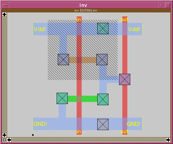
Your finished inverter design should look something like the figure:
To quit magic, type :q.
From the unix prompt you can type
check_magic_leaf_cell -T c035u -M 1 invto perform some basic checks on your design. In particular it will check that all your labels have been correctly drawn as line labels along the edge of the cell.
The requirements of this checking program may at first seem overly fussy, but cells which don't match these requirements will give at best unpredictable results when used in larger magic designs and cannot be ported to other design tools.
Details of the sort of problems identified by this program can be found on the Checking Magic Cells web page.
Although this design as it stands is complete, it is possible to improve it.
Transistor sizing
The minimum dimension transistors (W=0.5µm, L=0.35µm) used so
far will give the inverter a poor drive capability.
For this exercise an NMOS width of 0.8µm (this is chosen to be the
same as the minimum width of the ndc tile) and a PMOS width of 1.8µm
(this is chosen to be just over twice the NMOS width value)
will be used.
![]()
![]()
![]()
![]()
To connect the to the wider PMOS, larger contact tiles will be used,
this should result in lower contact resistance.
![]()
![]()
![]()
![]()
Were a slight adjustment in the position of a tile is required, it may be selected using the s macro and then nudged using one or more of the unit movement macros: q, w, e and r (q moves 1 unit left, w moves 1 unit down, e moves 1 unit up and r moves 1 unit right).
An alternative approach is to use the unit stretch macros for the nudging process (these are Q, W, E and R). The advantage of the stretch macros is that they stretch the paint behind the moved object thereby avoiding unintended gaps.
The unit stretch macros are used to tidy up the design,
firstly to re-align one of the ndc tiles
![]()
![]() and then to remove a notch violation.
and then to remove a notch violation.
![]()
![]()
![]()
N-Well Extension
In order to allow n-wells to connect between adjacent cells, the
n-well is extended to the left and the right edges of the cell.
![]()
![]()
Design Compaction
Producing compact leaf cells leads to smaller and cheaper ICs with better performance due to reduced parasitics.
Using the area select macro a and the unit stretch
macros Q, W, E and R provides
an excellent method of compacting the design.
Each selected area is nudged repeatedly until a design rule violation
is detected at which point the last nudge is undone.
![]()
![]()
![]()
![]()
![]()
![]()
![]()
![]()
![]()
![]()
Occasionally you will have to use stretch to increase
the size of the cell to remove a design rule violation.
![]()
![]()
Sometimes the compaction will create a notch violation
which can be removed by filling the notch before further
compaction is attempted.
![]()
![]()
![]()
![]()
![]()
![]()
Getting the Cell Boundary Right
The amount that the power and ground rails extend beyond the rest of the cell is constrained by the requirement to place cells side by side. Similarly the extension of the inputs and outputs above and below the power rails is related to the requirement to route signals above and below a row of cells.
An extension of 0.3µm for metal1 power and ground
rails and 0.25µm for
poly inputs and outputs is suggested for this exercise.
The area select and stretch process can be used shrink the design
to match the chosen extension values.
![]()
![]()
Note that the top extent of the nwell has been adjusted so that it coincides with the top edge of the power rail and hence it overlaps the nwt by the minimum value (0µm) specified in the desgn rules. Similarly the bottom edge overlaps the pdiff by exactly 1.0µm (again as specified in the design rules). Since the drawing of nwell is optional in magic, these design rules are not enforced by the checker, you must check them by hand.
Finishing Off
Having changed the position of the cell boundary it is
necessary to re-align the cell to (0,0) as before.
![]()
![]()
Although most signal tracks will narrow between contacts in order to reduce capacitance (c.f. the 0.5µm metal1 track between the 0.8µm wide drain connections to the two transistors), there is no need for power and ground tracks to narrow unless the narrowing results in an overall space saving.
For this reason we now increase the width of the power/ground
tracks that run to the to the transistor sources.
![]()
![]()
![]()
![]()
Use the :save command to save the cell without giving it
a new name.
![]()
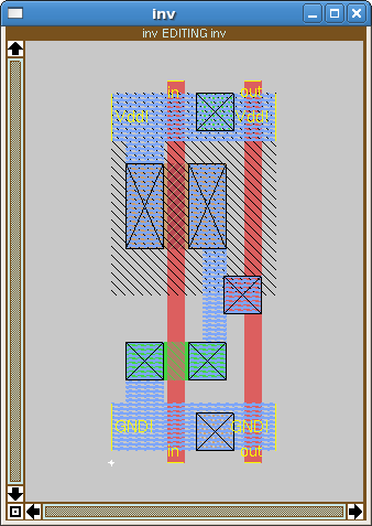
The result is a standard cell appropriate for use in more complex designs:
During the lab you have created a magic layout for a CMOS inverter cell. The transistor level circuit diagram and stick diagram for this cell are shown below:
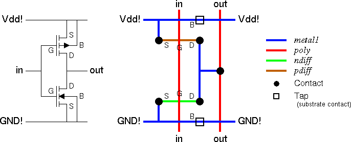
Note that the source (S), gate (G), drain (D) and substrate/bulk (B) connections for the PMOS and NMOS transistors are labelled on both diagrams.
As mentioned at the beginning of the lab, magic deals with abstract layers rather than true masks. The result is that a magic design looks very similar to the stick diagram from which it is derived.
When this abstract layers approach is combined with the magic on-line design rule checker, the result is a significantly simplified design process. This simplified process enables novice designers to produce functional and space efficient cell layouts with minimum effort (this explains why we use magic for cell design teaching).
Contacts
Although some magic abstract layers map exactly to a single mask layer (e.g. metal1), others map to multiple masks; in particular a magic contact between layer X and layer Y will map to mask data for layer X, mask data for layer Y and mask data to describe the contact windows that allow the two layers to connect.
Thus an ndiffcontact tile will map to metal1, ndiff and contact window:
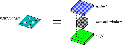
Magic will ensure that each of the two conductor layers overlaps the contact window by the correct amount to satisfy the design rules (so you don't have to worry about it).
Where a larger ndiffcontact tile is placed, magic will attempt to include multiple contact windows if there is sufficient space:
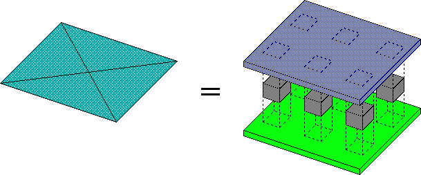
Note that we have multiple small contact windows because that way we get a lower resistance than with a single large contact window (strangely the current carrying capability is determined more by the sum of the perimeters of the windows than by the sum of the areas).
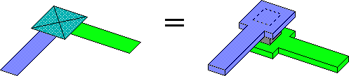
The overall result is that metal1 is generated wherever metal1 or any contact to metal1 is specified. Similarly ndiff is generated where ndiff or ndiffcontact is specified:
Diffusions
Each magic diffusion area will map to mask data to describe the active area, plus mask data to describe the appropriate implant. In the case of the pdiff abstract layer, magic generates active area and p-implant mask data with the p-implant mask overlapping the active area by an amount specified in the design rules:
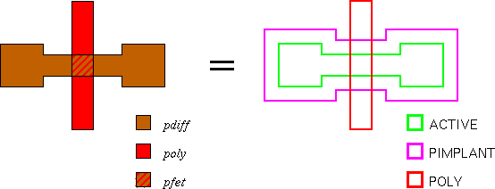
Note that an n-well mask will also be generated if you forgot to draw one. Unfortunately the autogenerated n-well mask seldom gives exactly the the n-well that you need so you should always draw your own.
Viewing the Real Masks
You can look at the mask data that will be generated by
magic using the :cif see command. For example to see all the
contact windows that will be generated within your inverter cell,
draw a box around the whole cell and type :cif see CON.
![]()
In order to clear the results of this command so that a new
:cif see command can be run type :feedback clear.
![]()
The "cif" names of the masks generated by magic for the "c035u" technology include:
| CIF name | Mask name | Description |
|---|---|---|
| NW | nwell | N-Well |
| AA | active | Active Area |
| POLY | poly | Polysilicon |
| PPI | pplus | P-Plus Implant |
| CON | contact | Contact Cut |
| M1 | metal1 | Metal 1 |
| V1 | v1 | Via 1 |
| M2 | metal2 | Metal 2 |
The following table summarises the magic commands and macros covered in this laboratory.
The table is incomplete. On your paper copy of this lab sheet you should fill in the long command and description for all the macros that have been used in this lab.
Details of the long commands for macros can be found in the file $CAD_HOME/lib/magic/sys/.magic. Corresponding descriptions can be obtained from this lab sheet or via the magic help command :help.
| Long Command | Description | |
|---|---|---|
| :load <cellname> | load a cell into a window | |
| :save [<filename>] | save edit cell on disk | |
| :q | exit magic | |
| :label <labelname> [<pos> [<layer>]] | place a label | |
| :grid <gridsize> | set size of grid | |
| :move to <x> <y> | move selection and box to (x,y) | |
| :cif see <ciflayer> | display CIF layer under box | |
| :feedback clear | clear all feedback info | |
| :help | print out synopses for all commands valid in the current window | |
| Macro | Long Command | Description |
| p | : | |
| y | : | |
| g | : | |
| G | : | |
| u | : | |
| U | : | |
| v | : | |
| z | : | |
| s | : | |
| a | : | |
| f | : | |
| q | : | |
| w | : | |
| e | : | |
| r | : | |
| Q | : | |
| W | : | |
| E | : | |
| R | : | |
| T | : |
Finish This Lab Sheet
You should finish this lab completely before the beginning of next the next lab session. This includes creation of a compact inverter design and checking it with the check_magic_leaf_cell program.
Ensure this Lab is Properly Documented
As documentation for the lab, you should have a paper copy of this lab sheet stuck in your log book annotated with your comments and observations. You should ensure that you have filled in the summary of commands and macros table in the review section.
A list of the magic macro commands can be found in the file $CAD_HOME/lib/magic/sys/.magic.
The full Magic Tutorials are available on-line.
You should read at least Magic Tutorial #2: Basic Painting and Selection in order to extend your knowledge of magic's facilities.
In addition Magic Tutorial #3: Advanced Painting (Wiring and Plowing) offers information on more advanced techniques including the very powerful plow command which can be used to speed up the compaction process.
The manual page for magic is also available on-line. Type the following at the unix command prompt:
man -s 1 magic
Mark Zwolinski
+Iain McNally
5-10-2015