CMOS Gate Array Design Exercise 2000
This year's exercise is to design a controller for a simple multi-cycle multipler. The controller should be versatile enough to cope with both signed and unsigned multiplications and variable precision arithmetic.
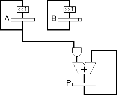
The simplest algorithm for multiplication involves repeated shift and add operations. In the figure below, the register A is initially loaded with the multiplicand and the register B is initially loaded with the multiplier while P which will contain the partial product is initially zero.
In the first cycle A is added to P if the least significant bit of B is '1'. A is shifted left while B is shifted right.
This process is repeated for N cycles where N is the number of bits in the operands. i.e. 8 times if A and B are 8 bit values.
The technique is simply one of long multiplication. Below you can see the long multiplication of two 8 bit values to produce a 16 bit result.
 Multiplicand         01010111              87
 Multiplier           00100101 x            37 x
                      --------             ---
                      01010111             609
                     00000000             261
                    01010111              ----
                   00000000               3219
                  00000000
                 01010111
                00000000
               00000000
              ----------------
 Product      0000110010010011
Dealing with a signed multiplicand is simply a question of sign extension of the value loaded into the A register:
 Multiplicand         11010111             -41
 Multiplier           00100101 x            37 x
                      --------             ---
              1111111111010111            -287
              000000000000000            -123
              11111111010111             -----
              0000000000000              -1517
              000000000000
              11111010111
              0000000000
              000000000
              ----------------
 Product      1111101000010011
Where the multiplier is negative it is necessary to perform a subtraction rather than an addition for the most significant (sign) bit:
 Multiplicand         11010111             -41
 Multiplier           10100101 x           -91 x
                      --------             ---
              1111111111010111              41
              000000000000000  +          369
              11111111010111   +         -----
              0000000000000    +          3731
              000000000000     +
              11111010111      +
              0000000000       +
              ----------------
              1111101000010011
              111010111        -
              ----------------
 Product      0000000010010011
In a real system the multiply unit is likely to be just one of a number of units sharing one or more common data buses. The following diagram shows the datapath of a multi-cycle multiply unit suitable for connection to a single system data bus:
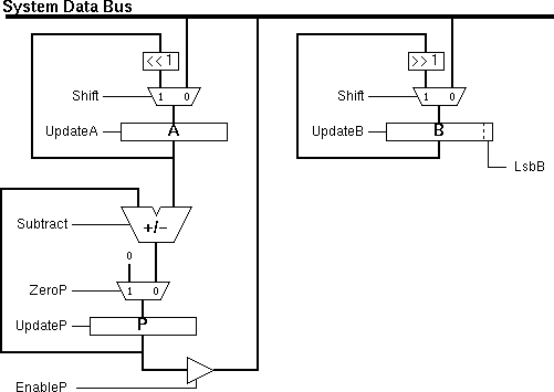
Note that in this datapath there is no AND gate to control the input to the Add/Subtract unit. Instead the UpdateP signal allows the output of the Add/Subtract unit to be ignored.
The following diagram shows a suitable sequence of control signals for the unsigned 8 bit multiplication:
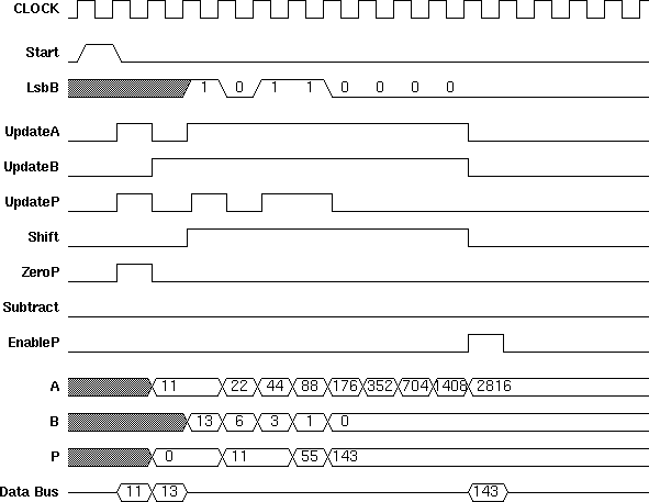
The multiplication is triggered by a Start signal external to the multiply unit. On the diagram you can trace the operation of the unit from the single cycle Start pulse, through the loading of A and B to the calculation and finally the output of P. Note that the system data bus is shown high impedance when it is not being used by the unit - this allows the bus to be used by other units as required.
The control signals generated by the controller are UpdateA, UpdateB, UpdateP, Shift, ZeroP, Subtract & EnableP.
LsbB is the feedback signal from the datapath to the control unit enabling the control unit to decide whether P should be updated with the result of the addition.
Your controller will generate the UpdateA, UpdateB, UpdateP, Shift, ZeroP, Subtract & EnableP control signals based on the Start input and the LsbB feedback signal.
In addition to these inputs there is an input Signed which tells the controller whether the operands are signed (i.e. whether the most significant bit of each operand is a sign bit - it does not tell us whether an operand is negative). The controller uses this information to decide when to set the Subtract signal to '1' which causes the Add/Subtract unit to perform a subtraction rather than an addition.
To cope with different widths of operand and different widths of datapath, the controller is also provided with two mode inputs Mode0 and Mode1. The following table shows how these signals effect the operation:
| Mode1 | Mode0 | Operation | |
|---|---|---|---|
| 0 | 0 | 0 | A and B are 8 bit values |
| 1 | 0 | 1 | A and B are 16 bit values |
| 2 | 1 | 0 | A and B are 32 bit values |
| 3 | 1 | 1 | In this mode the numbers of bits in A and B are unknown. Instead two more feedback signals are provided EmptyB & FullB. These signals allow the controller to detect when it has dealt with all the useful addition stages so that it can terminate the multiplication early. |
Your design for the frame synchronization unit must satisfy the following specification:
All designs must be fully synchronous. Major penalties will be incurred by teams who adopt asynchronous or quasi-synchronous design styles; as well as losing marks you will probably find that your design doesn't work.
A fully synchronous design contains no spurious state elements; no RS flip-flops, no transparent latches and no feedback paths within combinational logic blocks. The only state elements will be the the edge triggered D-types as supplied in the Gate Array library.
Inputs
A single clock signal with an active rising edge is common to all D-types. You should not attempt to connect this signal to any gate input or output which is not labelled CLOCK.
A single active-low asynchronous reset signal is common to all D-types, this input is used for initialization only. You should not attempt to connect this signal to any gate input or output which is not labelled nRESET.
This signal will go high to indicate that a multiplication is required. Care must be taken to reject a second start pulse while the multiplication is under way. Holding this signal permanently high should result in multiplications one after another.
This signal indicates that operands are signed. You may assume that this signal will remain stable for the duration of a multiplication operation.
These two signals define the mode as described above. Again you may assume that these signals will remain stable for the duration of a multiplication operation.
This signal is the least significant bit of the B register.
EmptyB is the logical NOR of all of the bits in the B register while FullB is the logical AND of these same bits.
These signals will only be valid in mode 3 (i.e. when Mode1=Mode0=1).
Outputs
These signals control the operation of the registers. Where the signal goes high for one clock cycle, the corresponding register is updated at the end of the clock cycle. This behaviour is as expected for synchronous designs.
Note that UpdateA and UpdateB will each cause the bus to be driven by an external source when the Shift signal is low. This means that it is not an option to set UpdateB permanently high.
These signals control the multiplexors within the datapath. Note that the registers will only be shifted/zeroed where the shift or zero is matched with an update signal. Note also that only one Shift signal is provided since the shift left of A is always coincident with the shift right of B.
This signal is set high for subtraction and low for addition.
This signal should go high for exactly one cycle after the multiplication is complete to allow the P register to drive the system bus.
This signal allows your system gracefully to reject requests for modes which are not supported by your hardware. See below for more details on relaxing the specification.
The only suggestion for this year is to include a programmable down counter as a separately testable module with a trigger input that goes high for one cycle to load the counter and a zero output to tell the rest of the system when the count is finished.
With the exception of the common inputs CLOCK, nRESET, Mode1 and Mode0 this block can easily be isolated from the rest of the system thus improving modularity and testability.
Remember that it is important to include as much testability as possible in order to get the best results out of the testing exercise next semester (many circuit breaks to improve observability and controllability and many test outputs to improve observability only).
During the testing stage, any separate blocks will be reconnected to give the originally specified functionality. With careful choice of signal names, this split circuit will simulate as if it was reconnected thereby assisting with design verification.
To cope with teams of differing capabilities, there are a number of ways in which the specification may be relaxed:
The minimum system should support mode 0 (8 bit) with both signed and unsigned operands.
The simulation will only work if the Unsupported output is asserted (logic '1') for modes 1, 2 & 3.
You can chose which other modes you will offer. Implementing mode 1 (16 bit) should be relatively straight forward once you have got mode 0 working provided that your down counter is a separate module, although mode 3 allows greater flexibility in operand width without large numbers of extra gates. Maybe you should consider mode 3 unsigned without mode 3 signed (which may cause extra problems).
You may find that you are unable to fit a full system on the Gate Array but you should remember that you are only competing against the other D2 teams - if no team manages it, then you are unlikely to lose marks as a result.
Making an informed choice
The choice of a circuit for implementation will be one of your most important design decisions for this exercise. In the initial stages you may like to produce outline designs for a number of different options. It is certainly possible that one or more of your initial designs will need more than the 67 available gate sites.
In choosing between designs, the key points to consider are:
Note that if you chose to relax the specification such as described above you must document this in both your interim and your final reports.
Iain McNally
19-10-2000