Designing for the CMOS Gate Array
Introduction to the CMOS Gate Array
Gate Arrays
The design of an integrated circuit is an expensive and time consuming task, requiring a high degree of skill from the designer. As a result, full custom IC design tends to be limited to high volume production chips.
Various strategies are used in order to reduce the cost of designing ICs, particularly the design turnaround time and the level of skill and experience required of the designer.
The gate array is one approach to the problem. Gate arrays provide a relatively cheap means of designing integrated circuits, particularly when only small numbers of chips are required.
In its simplest form the gate array consists of a regular array of uncommitted logic gates which can be connected together to form more complex digital systems. This is the process of customization. In many cases the customization of the gate array can be accomplished using a single metallization mask which connects together the gates as required.
Design costs are reduced because only one or two masks need to be generated for each new design, consequently the design is relatively simple and considerably less time consuming.
Fabrication costs are reduced because most of the masks are common to many designs, allowing mass production of uncustomized chips.
The CMOS Process
The CMOS Gate Array has been designed for the department's own 4um single layer metal CMOS process.
The masks which must be generated for this process are:
Mask 1 		NW  		 N Well 		 Pre-defined
Mask 2 		AA  		 Active Area 		 Pre-defined
Mask 3 		FI  		 Field Implant 		 Pre-defined
Mask 4 		NA  		 N-Channel Area 	 Pre-defined
Mask 5 		PA  		 P-Channel Area 	 Pre-defined
Mask 7 		P1  		 PolySilicon 		 Pre-defined
Mask 8 		CW  		 Contact Windows 	 Customized
Mask 9 		M1  		 Metal 			 Customized
The M1 metal mask is customized to produce the tracks for intra-gate and inter-gate connections.
The CW contact window mask defines where the M1 mask connects to the circuit elements defined on the uncustomized chip.
Note that Mask 6 (BA) is not used in this process.
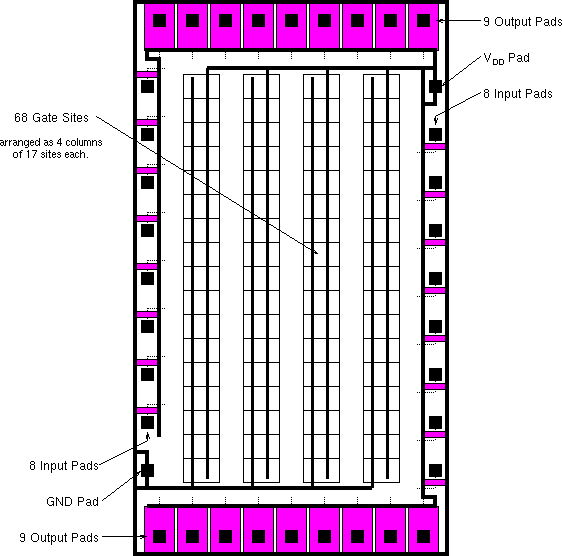
Layout of the uncustomized Gate Array
The uncustomized CMOS Gate Array has:
- 68 gate sites arranged in 4 columns of 17.
- 16 input pads with basic diode protection arranged down the left and right sides of the chip.
- 18 output pads with associated buffer circuits arranged across the top and bottom of the chip
The layout of these items is shown below:
Customization of the gate sites
Each gate site contains 12 transistors ( 6 N-type and 6 P-type ). These transistors can be connected together in a number of different ways to produce different gates.
To aid in the customization 13 gate overlays have been provided. Not surprisingly, when correctly placed over a gate site a gate overlay will create a gate.
Some gate overlays are full size overlays and occupy a whole gate site, these are:
		NAND4 		4 input NAND gate
		XOR2 		2 input XOR gate
		XNOR2 		2 input XNOR gate
The remaining overlays are half size overlays, these are:
		NAND2 		 2 input NAND gate
		NAND3 		 3 input NAND gate
		NOR2 		 2 input NOR gate
		NOR3 		 3 input NOR gate
		AND2 		 2 input AND gate
		OR2 		 2 input OR gate
		INV 		 Inverter
		GND 		 For connection to Logic 0
		VDD 		 For connection to Logic 1
		X_X 		 For feedthrough connections
It is possible to place two half size gate overlays over a single gate site provided that the lower of the two is placed upside down (i.e. reflected in the x-axis).
N.B. You are strongly advised not to attempt to design your own gate overlays as this would make my job much harder!
Macro Cells
As well as the standard gate overlays, you are provided with an overlay for an edge triggered D-Type flip-flop.
The D-Type design is shown below as a schematic with four 3-input NAND gates and two 2-input NAND gates.
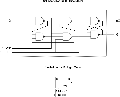
The corresponding DFF overlay contains four NAND3 overlays and two NAND2 overlays together with a number of tracks and contact windows to perform the necessary interconnections.
The DFF overlay is described as a macro because it is not a single flat cell since it contains references to other cells.
With careful thought it is possible to design your own macros for sub-circuits within your design.
Routing
Any area not occupied by anything else is taken up by routing channels. There are five vertical routing channels and two horizontal routing channels.
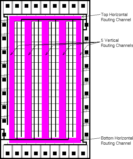
Pads and gates are joined by tracks drawn in metal (M1). Where a track needs to cross another track or power rail, there are polysilicon underpasses (well over a thousand of them) pre-defined on the Gate Array. Connections are made to the polysilicon underpasses by etching contact windows in the oxide layer which would otherwise insulate the polysilicon from the metal. These are defined as rectangles on the CW mask layer.
Feed Through Routing
Although it appears that horizontal routing is restricted to the two horizontal channels at the top and bottom of the cell, this is not the case.
An examination of the gate overlays shows that many gates have two extra terminals (marked X). These terminals make use of a polysilicon underpass built into the gate site in order to pass a signal under the power rails running through the site. Thus we have a feed through connection allowing horizontal routing through the gate.
Note that the routing problems are significantly reduced by the duplication of most gate terminals at the left and right of each overlay.
Circuit Design and Simulation
Design Constraints
The first stage of the design is the schematic diagram of the circuit. The elements of the circuit diagram should be symbols from the set below:
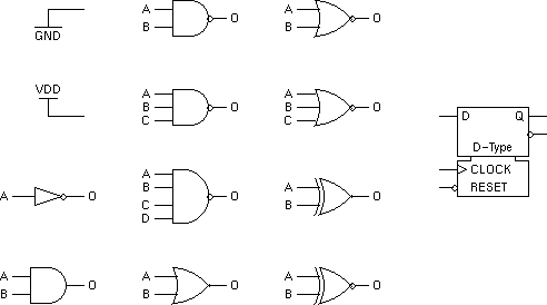
Each symbol corresponds to one of the gate overlays.
Schematic Capture
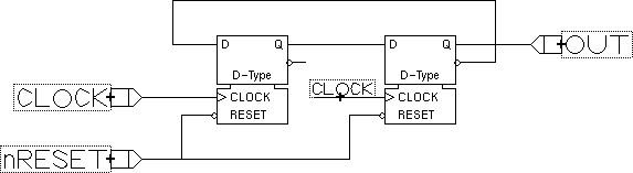
The following is a schematic diagram for a simple sequencer circuit as you might draw it on paper. In addition to the symbols shown above it has INPAD and OUTPAD symbols at its inputs and outputs. These symbols will map to the input pads and output pads of the Gate Array.
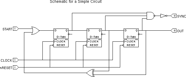
The first stage of the CAD design cycle is to capture the schematic such that it can be checked and simulated.
It is anticipated that you will go through several iterations of the schematic capture process before you are satisfied with your design.
Since schematic capture is very much faster than layout for the Gate Array, extra time spent here in order to ensure a correct and efficient design will save you considerably more time in later stages.
Notes on the creation of Icebox Schematics
- Starting Off
You should use H:\design_2\schematic as your design directory, CGA SCHEMATIC as technology and cgaSch.gds as reference library.
For details on the use of reference libraries with Icebox together with
tips on choice of cell and library names, see appendix 1.
- Symbol Placement
With Icebox NT 2000, Place Cell is performed as a drag and drop operation from the library(s) window to the edit window.
Select the required library, cgaSch, and then the required cell, e.g. NAND2 from the library(s) window and drag it into the edit window.
- Wiring
All wires are drawn as paths on the wire layer; WIRE.
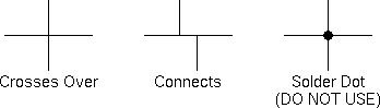
Note that normal rules apply for the interpretation of wire intersections.
Although some CAD tools permit the use of a "solder dot" to connect wires
which would otherwise appear to cross, this is considered poor style since
small solder dots are often lost during photocopying while large solder dots
obscure the picture. You should not use solder dots in your schematics.
- Labelling
All labels are drawn as text items on the label layer;
LAB.
Labels should contain only letters; {A-Z,a-z} and numbers; {0-9}.
Although labels may also include a single underscore character; {_}, this should be avoided at this stage since it has a special meaning which will be explained later.
Labels must start with a letter.
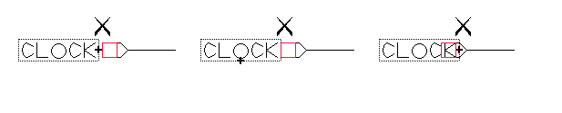
- Wire Labels
In order to label a wire you must place it with its origin over the wire.
The origin of the text is the large white crosshair cursor visible during text placement.
Thus a Centre-Justify-MIDDLE label is placed with its centre over the wire, while a Centre-Justify-BOTTOM label sits neatly on top of a horizontal wire allowing the text to be read easily.
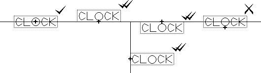
If the origin of the text does not touch the wire then the wire is not labelled regardless of the proximity of the label to the wire.
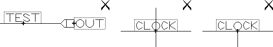
- Pad Labels
A labels is placed with its origin over the red square of the pad
symbol in order to label the pad.
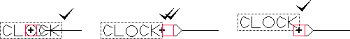
Conversely if the origin does not touch the red square then the pad is not labelled.
- Join by Name
All wires and pads with the same label are automatically joined. If used with care this facility can improve the readability of complex schematics.
- Labelling Errors
- It is an error to place two different labels on the same net.
- It is an error to label a crossover since it is unclear which net is being labelled.
- It is also an error to label a junction since the label must attach to a single wire segment.
Finished Schematic
The following shows a complete schematic for the simple sequencer drawn using icebox.
Netlist Extraction
Netlist extraction converts your schematic into a netlist text file which can be understood by the simulator. It also helps to identify any errors in the construction of the schematic.
A remote netlisting utility is available for those using Icebox on the department's Windows 2000 machines in Zepler.
- Ensure that you have saved your design to disk (since the netlist will use the disk copy of your file) - use Save Working Library As... from the File menu.
- Select Remote CAD Tools from the Tools menu.
The default settings should be fine although you may like to change the Team/User field to show your team name; e.g. teamz.
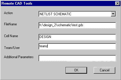
- After hitting OK a new window will be invoked and you will be asked to supply username and password for the CAD server. If you are working as a team, remember that it must be the owner of the H: drive on the PC who logs onto the server, otherwise the server will see no files and take no action.
During the remote netlist procedure you may see error and warning messages most of which can be ignored - the key information will be returned to you in the netlist file.
The time taken to complete the procedure will depend on the load on the server; please be patient.
- If all goes well the results are returned in the netlist file; NETLIST_S.TXT.
- NETLIST_S.TXT is a simplified netlist of the design in terms of library gates.
Where the netlist is successfully created, it is displayed immediately via the Notepad program.
The following is the netlist for the simple sequencer described in this document:
   //Netlist for cell design from library teamz

   //Design extracted ok - with warnings

   //\o Warning: Pin "nQ" on instance "I4": floating output.
   //\o Warning: Pin "nQ" on instance "I5": floating output.
   //\o Warning: Pin "nQ" on instance "I6": floating output.
   //\o There were 0 errors and 3 warnings found in "teamz design schematic".

   dtype #1 I5 ( OUT , d5nq , CLOCK , nRESET , d6q );
   dtype #1 I6 ( d6q , d6nq , CLOCK , nRESET , d7q );
   dtype #1 I7 ( d7q , d7nq , CLOCK , nRESET , or8 );
   or #1 I8 ( or8 , START , xor11 );
   nand #1 I9 ( nand9 , d7q , d6q , OUT );
   not #1 I10 ( SYNC , nand9 );
   xor #1 I11 ( xor11 , OUT , d6q );
- Netlist interpretation
Boolean gates are indicated as:
function #1 instance ( out, in1,
in2, ... );
Whereas d-types are indicated as:
dtype #1 instance ( q, nq clock,
notreset, d );
If not explicitly labelled, the name of a net is derived from the gate that drives it:
e.g. nand9 is driven by nand gate instance I9.
- Netlist errors
The netlist above lists three warnings generated during extraction. Each represents an unconnected output from a D-Type. Since each D-Type has two outputs this warning can be ignored. In general an extraction warning will be the result of a mistake in your schematic.
In addition to extraction warnings and errors, the netlist will list obvious errors such as floating inputs and shorted outputs. You should correct these errors and re-netlist before proceding to the simulation stage.
- Where an error has occurred during extraction the file EXT_S.GDS may be created. You may like to consult this file if you are unable to track down netlist errors based on the NETLIST_S.TXT file only.
- Use Icebox to examine the updated version of your design within EXT_S.GDS. Errors are indicated by shapes on the extraction error layer;
ERR. You may wish to turn off all other layers in order to track down these errors.
Simulation
Having successfully extracted a netlist, you know that you have designed a circuit, with the aid of simulation you will hopefully be able to predict whether the circuit will work.
A remote simulation utility is available for those using Icebox on the department's Windows 2000 machines in Zepler.
- Verilog
The simulator we will use is Verilog-XL which is designed around the
Verilog Hardware Description Language. It is used widely for design
specification, design synthesis and design verification.
Due to the time constraints on the exercise, we cannot expect you all
to read extensively about Verilog, so we have created a very simple
turnkey system which will give good results for a good design. In order to
get more out of the system and probably improve your overall design mark you
will have to do some research into the use of the simulator.
- Exceed
Exceed allows "X-Windows" programs from the CAD server to display graphical results on your local PC.
Ensure that "Exceed" is running on the PC before initiating your simulation.
- Remote Simulation
Simultion is initiated from the Remote CAD Tools dialogue.
The Remote CAD options are:
- Action: SIMULATE SCHEMATIC
- Additional Parameters: -exceed -simulate test
The result should look somthing like this:
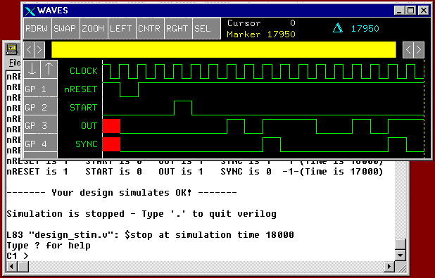
Having confirmed that your design simulates OK (or otherwise), typing "." in the Tera Term telnet window will terminate the simulation and return you to Icebox.
- Specifying the simulation
A simulation will depend on a stimulus file that defines how inputs are driven and which outputs are viewed. The test simulation shown above works for the example circuit described in this document. Other stimulus files are required for other circuits. In general the D2 design should be testable using the final stimulus. This is selected by specifying the following remote CAD options:
- Action: SIMULATE SCHEMATIC
- Additional Parameters: -exceed -simulate final
- More?
The documentation here is intentionally sparse. More information on Verilog simulation is available on the
CAD Tools and Techniques homepage at
http://www.ecs/~bim/notes/cad.
Testability
Before committing your design to silicon you must consider testability. With simple designs such as those implementable on a Gate Array it is relatively easy to say whether the circuit works but much harder to determine why a circuit doesn't work.
Faults in the finished design will be of two types :
- Design Faults
These faults are created by you at the design stage - maybe you'll miss out a contact window or connect a track to the wrong terminal of a gate.
These faults will be systematic - if the contact window is missing then the same fault will exist on all samples of your chip.
Note that a successful simulation is not a guarantee of a chip that meets the specification. It doesn't even guarantee that chip will work in the limited manner tested by the simulation. The only definitive test is done once the chip has been fabricated.
- Processing Failures
Processing failures may occur due to misalignment of masks or contact windows etched too large/small.
These faults are likely to be random, different samples may exhibit different faults.
Following fabrication you will have to test a number of samples of your design. Your task will be to prove that your design is correct. Given that there are errors in your design, you will have to identify them and prove that the rest of the circuit still works.
There are two techniques that you should use to increase the testability of your design :
- Division of circuit into testable blocks.
- Addition of ad-hoc testability.
Taking the simple sequencer circuit as an example we can see how testability can be improved :
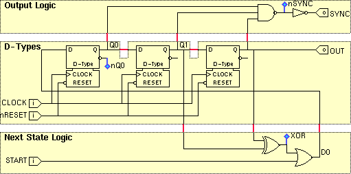
Division of circuit into testable blocks.
The circuit has been divided into three blocks; D-Types, Next State Logic and Output Logic. Each sub-circuit has its own inputs and outputs in order to maintain independence.
During testing it is possible to re-connect the blocks to check overall functionality, or keep the blocks separate in order to isolate faults and prove functionality of correctly designed blocks.
Addition of ad-hoc testability.
Certain internal nodes have been connected to output pads such that their state can be monitored. This will also help in the isolation of faults and in proving the functionality of correctly designed blocks.
You should make your design as testable as possible. The major limit on testability is the availability of I/O pads.
If you have more than a few unused I/O pads then your design is not testable enough.
Some of the most common systematic errors result in the failure of all d-types.
How much of your design will you be able to demonstrate if all your d-types fail?
Schematic Annotation and Pad Naming
Each symbol in the schematic diagram should be uniquely labelled for ease of
identification.
These identifiers should be added as text items on the text layer;
TXT.
At this point we must also ensure that the inputs and outputs have unique names (even where it is intended to re-connect them after fabrication). To help with netlisting and simulation we
use the convention that signal uvw_xyx is an input signal which will be driven
by the output signal uvw.
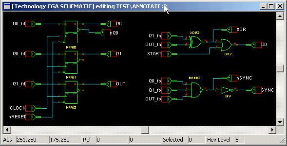
The following figure illustrates this process for our simple sequencer:
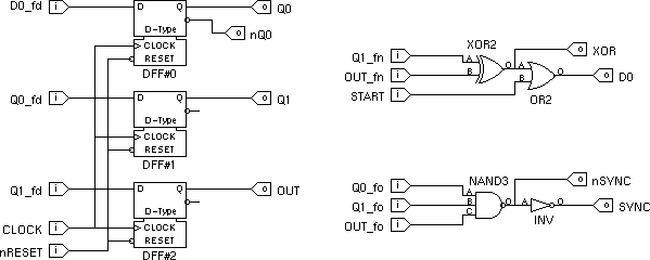
Points to note:
- The D-Types are numbered for easy identification, while the
XOR2 gate is simply labelled XOR2 since there is only one such gate
in the design.
- The input pad labelled Q1_fn is clearly distinguished from the input
pad Q1_fo and Q1_fd. From the convention described above we can
infer that each of these input pads will be driven in the final circuit from
the output pad Q1.
-
The information from this diagram will relate exactly to the final design.
Tracing a single node we see that;
the output O of the XOR gate XOR2
is connected to the input A of the OR gate OR2 and also to the output pad XOR. This will be the exact configuration on the Gate Array.
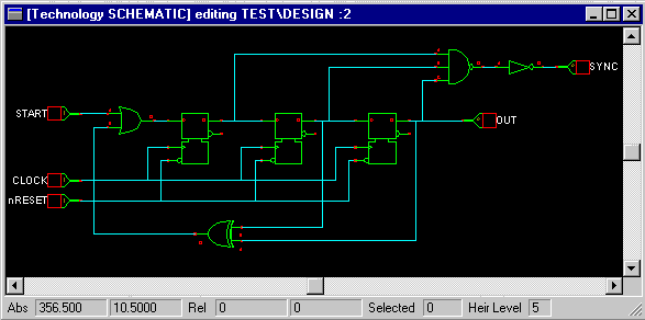
Finished Schematic with Testability and Annotation
The following shows a complete schematic for the simple sequencer drawn using
icebox.
This schematic can be netlisted and simulated as before. Provided that the
rules and conventions are obeyed, the simulation results will be unchanged.
Layout
Preparation
CGA Placement Template
To aid with the gate placement and i/o allocation a template has been created. Its usage is best illustrated by example:
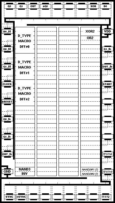
The proposed position of each gate and each pad from the annotated schematic is marked on the template. The unique gate and pad names are used to avoid ambiguity. Gates and pads which will be interconnected are placed in close proximity.
Notes:
- different sized gate overlays are shown taking up different proportions of a gate site.
- there are 14 un-allocated input pads (8 on the left and 6 on the right) and 17 un-allocated output pads (9 on the top and 8 on the bottom).
- an input pad cannot be used as an output nor can an output pad be used as an input!
- there are two test gates in the bottom right hand corner of the array which will be present on all chips.
Starting Icebox for Gate Array Place & Route
You should use H:\design_2\layout as your design
directory, CGA LAYOUT as technology and cgaLib.gds
as reference library.
For details on the use of reference libraries with Icebox together with
tips on choice of cell and library names, see appendix 1.
Gate Placement
Armed with your completed CGA placement template, you are now ready place the gate overlays on the Gate Array.
- Edit cell DESIGN.
If you don't have an edit window open for cell DESIGN, open one now.
- Place the ARRAY base part from the cgaLib library.
With Icebox NT 2000, Place Cell is performed as a drag and drop operation from the library(s) window to the edit window.
Select the required library, cgaLib, and then the required cell, ARRAY from the library(s) window and drag it into the edit window.
Accurate placement is all important here, ensure that you drop the ARRAY part exactly at the origin (0,0).
If you've got it wrong, select the newly placed ARRAY, delete it and start again.
- Place all the gate overlays onto the new cell.
For each gate overlay you must select the required cell from the cgaLib library and then place it over the appropriate gate site. Remember to reflect any overlay which is to occupy the bottom half of a gate site. If you select the custom snap grid for gate placement you may find the task easier as it forces you to align the gate overlay with an appropriate gate site.
Both the reflection and snap grid selection are performed via the place cell properties card.
- Save the working library with a suitable name.
The required command is Save Working Library As. When prompted for the name you should type in a new name rather than select one from the list. Remember to increment the version number so that you can return to a previously good file in the event of subsequent problems.
Labelling
Text may be added by selecting the appropriate mask layer and using the Create Text command.
- Labelling the I/O pads.
Again, you will need to consult your CGA placement template, this time to extract the pin
names.
Pin names should contain only letters; {A-Z,a-z}, numbers; {0-9} and the underscore character; {_}. Pin names must start with a letter.
Note that the underscore character {_} should be used only to indicate a connection which has been broken to improve testability. Using the underscore in any other pin name will cause the simulation to fail.
Pin names should be added as text items on the LAB layer. They should be
added using default Ariel font using centre/centre justification and a font size
of about 50 units (1 unit = 1um).
All font and justification selection is performed via the text properties card.
The origin of the text must be placed centrally over the metal of the relevant pad.
- Additional Text.
If you wish to add extra text for your own use, you should use the TXT layer rather than the LAB layer.
Since they don't modify the function of the circuit, neither of these layers will exist on the finished design. Text on the LAB layer will be used by the netlister to provide you with additional feedback before your design is fabricated.
- Do not create text on any other layer!
Routing
For this operation you should have a copy of the fully annotated circuit diagram. You may find it useful to tick off connections and nodes as you route them.
- Route each node in full.
Select a node to route. For best results route the clock signal and other global signals first!
If you always complete the routing of one node before going to the next you will make fewer mistakes and will get a more efficient layout.
Node routing is simply a matter of defining the metal tracks and contact windows that make up the node.
- Select M1 as the current mask layer.
- Draw one or more Paths, Polygons or Rectangles to represent the required area of metal.
- Select CW as the current mask layer.
- Draw one or more Rectangles to represent the contact windows for connection to the polysilicon underpasses
On completion of each node its connectivity should be checked. The errors to look out for are:
- Forgetting to place a contact window.
- Shorting two nodes by using the same polysilicon underpass twice.
- Leaving small 1um or 2um gaps between sections of track which can only be spotted at high magnification.
Further details on design rules and routing styles are given in the next section of this document.
- Save the working library regularly.
The routing process is likely to take a long time. Regular saving of your work could save you a lot of time.
If you change the library name regularly it will allow you to backtrack in the event of errors. If you only use one library name you will find it very easy to copy a corrupted version on top of your only backup.
Design Rules
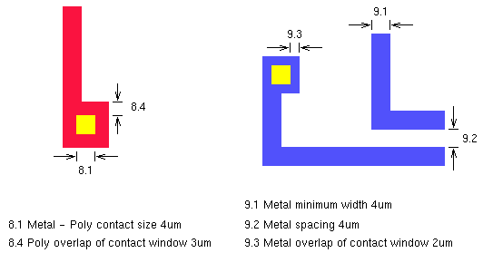
Certain Design Rules must be obeyed in order to ensure successful manufacture. The design rules that effect routing on the Gate Array are:
You should aim to layout tracks in a logical manner in order to avoid design rule violations.
Remote design rule checking is available for those using the department's Windows 2000 machines in Zepler.
- Select Remote CAD Tools from the Tools menu.
The default settings should be fine to perform a DRC LAYOUT although you may like to change the Team/User field to show your team name; e.g. teamz.
Remember that it must be the owner of the H: drive on the PC who logs onto the
remote CAD server.
- If all goes well the results are returned in the files, DRC.TXT and DRC.GDS.
- DRC.TXT is the log file from the design rule check, including a summary of the numbers of different types of error. This file is displayed immediately in a copy of Notepad.
- Use Icebox to examine the updated version of the DESIGN cell within the DRC.GDS. Design rule errors are indicated by shapes on the DRC layer. You may wish to turn off all other layers in order to track down these errors.
- As well as the (minimum dimension) design rules shown above, the DRC program will also highlight the following errors:
- Floating metal tracks.
All metal tracks must connect either to a gate overlay or a polysilicon underpass.
- Misplaced contact windows.
All contact windows must be covered by metal.
All contact windows drawn by you should connect to polysilicon.
- Contact Window spacing.
Two contact windows must be at least 4um apart.
- Metal/Contact Window outside routing channels.
All the shapes you draw on the metal and contact window masks should be inside the routing channels. Only gate overlays should overlap with the gate sites.
You may like to experiment with the DRC by breaking these design rules to check that they are spotted.
- These design rules are only a small subset of the full rules. All designs will be fully checked before fabrication.
- Passing the design rule checker is no proof of a functioning chip!
Routing Styles
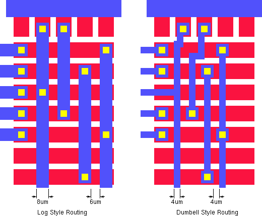
There are two different routing styles which lend themselves to use on the Gate Array.
The first, log style, makes use of the regular layout of the
polysilicon underpasses on a 14um grid.
Metal tracks are drawn as 8um wide paths with a gap of 6um between adjacent tracks.
Where a contact is required the CONTACT cell is placed rather than explicitly drawing metal and contact window rectangles.
All this can be done on a very coarse 14um snap grid making this routing quick and simple. Being correct by design it is very easy to spot any design rule errors.
For these reasons, log style is the preferred style for this exercise.
With the alternative dumbbell style there is room for more tracks in
the routing channels. Tracks can be as thin as 4um (widened to 8um around the
4um contact window) with a metal to metal minimum spacing of 4um.
When using this style the snap grid must be reduced to 2um making the task much more difficult. You should only use this style when space is restricted.
Netlist Extraction
Netlist extraction helps you to debug and hopefully simulate your design BEFORE it is fabricated.
- Netlist extraction is invoked in the same way as design rule checking. Simply select NETLIST LAYOUT from the available functions on the Remote CAD Tools form.
- If all goes well the results are returned in the files, NETLIST.TXT, PINOUT.TXT, ASSIGN.TXT and EXT.GDS.
Where they have been successfully created, these three files are displayed immediately via the Notepad program.
- EXT.GDS may be created where extraction has failed. As with DRC.GDS, error information is stored on the DRC layer.
The following is the netlist for the simple sequencer described in this document:
      //Netlist for cell final from library teamz

      nand #1 I1 ( nSYNC , Q0_fo , Q1_fo , OUT_fo );
      not #1 I2 ( SYNC , nSYNC );
      dtype #1 I3 ( OUT , d3nq , CLOCK , nRESET , Q1_fd );
      dtype #1 I4 ( Q0 , nQ0 , CLOCK , nRESET , D0_fd );
      dtype #1 I5 ( Q1 , d5nq , CLOCK , nRESET , Q0_fd );
      or #1 I74 ( D0 , XOR , START );
      nand #1 I75 ( nand75 , TESTnR , TESTQ );
      nand #1 I76 ( TESTQ , TESTnS , nand75 );
      xor #1 I77 ( XOR , Q1_fn , OUT_fn );
Boolean gates are indicated as:
function #1 instance ( out, in1,
in2, ... );
Whereas d-types are indicated as:
dtype #1 instance ( q, nq clock,
notreset, d );
The name of a net is derived from the gate that drives it:
e.g. nand75 is driven by nand gate instance I75.
unless it is connected to an external pin, in which case it takes the name of that pin.
e.g. START is connected to input labelled START.
Interpretation of Netlist Errors
Obvious errors such as floating inputs and shorted outputs are explicitly indicated in the netlist.
The following is the netlist for the simple sequencer including some rather less obvious errors:
      //Netlist for cell design from library teamz

      nand #1 I1 ( nSYNC , Q0_fo , Q1_fo , OUT_fo );
      not #1 I2 ( SYNC , nSYNC );
      dtype #1 I3 ( OUT , d3nq , nRESET , CLOCK , Q1_fd );
      dtype #1 I4 ( Q0 , nQ0 , nRESET , CLOCK , D0_fd );
      dtype #1 I5 ( Q1 , d5nq , nRESET , CLOCK , Q0_fd );
      or #1 I74 ( D0 , xor77 , START );
      nand #1 I75 ( nand75 , TESTnR , TESTQ );
      nand #1 I76 ( TESTQ , TESTnS , nand75 );
      xor #1 I77 ( xor77 , Q1_fn , OUT_fn );
Less obvious errors include:
- Unconnected gate outputs
the output of the xor (xor77) is not connected to the XOR output pin.
- Miswired inputs
the CLOCK and nRESET inputs of all d-types are swapped, this is only obvious if you know the order in which d-type inputs should be listed.
- These returned netlists are not perfect, it is the price you have to pay for
their simplicity.
- The netlist should be correct for a well laid out design, but it may not be a true representation for a lesser design.
Simulation
The procedure for layout simultion is identical to that of
schematic simulation with the exception that the
SIMULATE LAYOUT option should be chosen in place of
SIMULATE SCHEMATIC.
Since the layout should be node for node identical to the annotated schematic,
the simulation results should be unchanged.
Outline Timetable
- Introductory Meeting
The introductory meeting kicks off the project with a talk and hopefully a demo.
The intention is to give you an overview of the design & implementation stages
of the exercise.
The meeting also gives you a chance to ask questions and a chance to find the other
people in your team.
- Team meetings and design suggestions
Between the introductory meeting and the first Icebox sessions you should meet
with your team to discuss strategy and to come up with one or more initial
design ideas.
- Supervised Introductory Icebox Session
Your team will be scheduled for a single morning or afternoon supervised introductory
icebox session. Your team should send four people (your Icebox team) to this session.
Two people will work through the layout, DRC, netlist and simulation of the test
design described in this document. The other two will work on schematic capture for
the same design.
Please do not expect to get any real layout or schematic work done in this session -
if you try to do anything more complicated than the test exercise you will not get
through all the design stages within a single session and this supervised session will
be wasted.
- Unsupervised Working
As with other design exercises, you are expected to complete the majority of
the work without close supervision.
To complete the work in the limited time available,
you may book departmental NT workstations at any time that they are not
booked for a class or alternatively you can use Icebox at home
(if your PC runs Windows 2000 or NT).
In fact you should aim to finish the exercise in time for your second
scheduled lab session (this will enable you to get the most out of the
second session and will allow for inevitable slippage in your timetable).
Teams who are having difficulty with designs that won't simulate or give
strange results (maybe you just can't understand the specification) should
seek help early.
There is not much hope of you meeting the deadline if you wait to ask for
help until the day before handin.
- Scheduled Help Session
The second scheduled session should help you to finish off the design,
possibly helping you with advanced simulation features in order to debug
your layout. If you have done particularly well you may only need help
with production of simulation plots for your report.
All we can say is that you'll probably need some help at that stage of
the project, so we've booked the lab and will be there to offer assistance.
- Submission
Design submission is automated using the department's web based handin system at
http://handin.ecs.soton.ac.uk.
Three .gds files must be submitted:
- Schematic1.gds an icebox schematic library containing a cell called
DESIGN which is the schematic of the full system before the addition of
testabitity.
- Schematic2.gds an icebox schematic library containing a cell called
DESIGN which is the schematic of the full system with testability and
annotation.
- Layout.gds an icebox layout library containing a cell called
DESIGN which is the design that you wish to get fabricated.
Various checks will be performed automatically on the files you submit.
In particular your layout must pass basic DRC and netlist checks before it can
be accepted for fabrication.
Note that the cell name must be DESIGN in each case so that the
automatic checks can operate.
You should receive two e-mails as a result of the submission.
The first is your Coursework Hand-in Receipt from helpdesk.
The second is the result of the various acceptance checks.
If the submission is rejected then you must correct the mistakes and
re-submit.
Please allow plenty of time in your schedule to allow for re-submission.
If you are having difficulty getting through the design submission process
seek advice early.
END BIT
Advice
- Read the whole of this document before starting with Icebox. (O.K., so its probably too late to tell you this.)
- Browse through the Icebox web page to find information on commands not mentioned in this document.
- Read this document again as you work with Icebox. (There is a lot of information here.)
Information
- This document was written by me, Iain McNally.
- The Icebox NT 2000 software has been developed by John Clark.
- John Clark and I will be available throughout the project to offer our expertise.
You can get hold of me by e-mail: bim@ecs.soton.ac.uk
Or in person: Mountbatten room 2031 Tel. x23124
Please check my timetable on the Web to avoid a wasted journey:
http://www.ecs/~bim/timetable.html
You can get hold of John by e-mail: jgc@ecs.soton.ac.uk
Or in person: Zepler room 2221 Tel. x22826
- All mistakes in this document are my responsibility. All mistakes in your chip are your responsibility.
Web Resources
GOOD LUCK!