Integrated Circuit Engineering 2
This lab is provided to help you to remember what you knew of L-Edit and the Scalable CMOS technology. The lab will cover in particular the use of good hierarchy to create design modules and the use of T-Spice simulation to characterize your designs. It is hoped that by giving examples which use good design practice it will encourage you to use similar practices within your own designs.
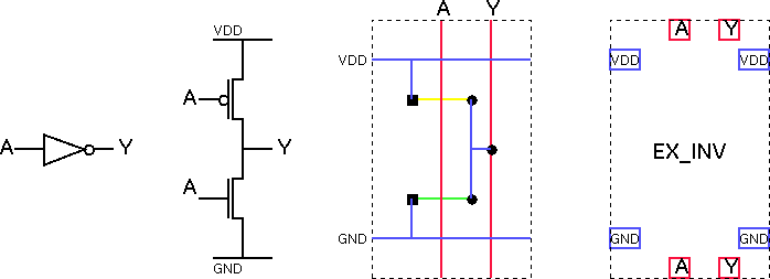
Four representations of the inverter, EX_INV, are shown below:
The first two are the symbol and the transistor level circuit schematic of the inverter. The third is the stick diagram for the inverter using the standard colour coding:
| Red | Polysilicon |
| Green | N diffusion |
| Yellow / Brown | P diffusion |
| Blue | M1 |
| Purple (Magenta) | M2 |
| L.Blue (Cyan) | M3 |
| Black | Contacts & Taps |
The stick diagram represents the layout in a shorthand form, allowing us to identify the arrangement of transistors, conductors and contacts. Note that an N transistor exists where Polysilicon (red) crosses N diffusion (green) while a P transistor exists where Polysilicon (red) crosses P diffusion (yellow/brown).
The last of the representations is known as a layout abstract or simply a black box representation. When we draw gate level circuit schematics we use the symbol for the inverter since we are not concerned with the implementation of the inverter only its function. Similarly when we draw a module layout including inverters and other leaf cells, we prefer to use the abstract representation of the inverter since it tells us exactly what we need to know in terms of the location, name and conductor type of each input and output together with an outline which tells us the extent of the cell (without the clutter created by including internal detail).
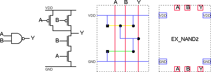
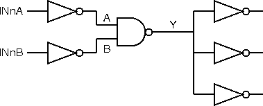
The corresponding representations for the two input NAND gate, EX_NAND2, are:
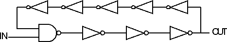
The third cell is a ring oscillator module, EX_RING, constructed from 9 leaf cells (8×EX_INV, 1×EX_NAND2) plus interconnect.
The stick diagram for the ring oscillator uses the abstract representations of the leaf cells:
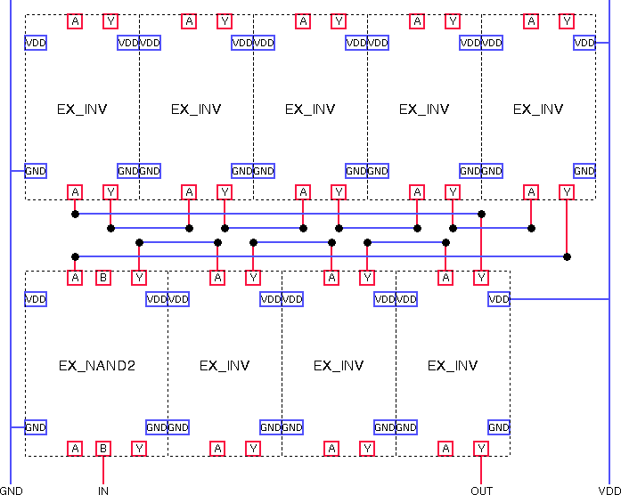
Note that the wiring of VDD and GND is implicit where two leaf cells are butted within a row since the VDD and GND ports of one abstract butt against those of the adjacent abstract. Note also that this module uses a strict two conductor routing strategy with metal 1 horizontally and polysilicon vertically (the exception being the vertical power rails to the left and right which must always be in metal).
Select the EX_INV window to fill the available space (Maximize). Hitting the [Home] key will centre the cell within the window. Now turn off the visibility of boxes (View->Objects->Boxes). You should be left with only the ports which make up the abstract view of the cell. Note that the A and Y ports are in red since they were drawn on the Poly layer while the VDD and GND are in blue on the Metal1 layer. If the ports are drawn on the wrong layer they will not be recognised by the extraction tool and simulation would fail. The last port is the cell outline which has been drawn on the Cell Outline Layer. If you select this outline or another of the ports, a description of the selected item will be displayed at the bottom of the main L-Edit window.
Re-enable the visibility of boxes (View->Objects->Boxes). In this design all of the cell exists within the cell outline. In many designs certain masks such as the N Well and the N and P Select regions may extend beyond the cell outline. One of the major tasks in cell design is to ensure that neither masks contained within the outline nor masks which overlap the outline cause DRC errors when interacting with adjacent cells.
Restore the EX_INV window to its smaller size (Restore Down) and maximize the EX_RING window. The view that you have of the layout shows masks within the top level cell (EX_RING) but only the abstract representations of the leaf cells (EX_INV & EX_NAND2). We say the view hierarchy level is set to 1.
Set the view hierarchy level to 2 (View->Hierarchy Level->View Hierarchy Level...) this will allow you to see the insides of the leaf cells. It is now less clear which elements (e.g. Metal 1 tracks) are in the top level cell and which are in the lower level cells. Also the function of each sub-cell, as suggested by its name, is less obvious.
Set the view hierarchy level back to 1. You will find you have to make use of different view hierarchy levels at different stages in the design. In general when placing and routing cells to make up a module you should use level 1.
Open the EX_RING cell and initiate the extraction process (Tools->Extract). The default options in the extraction dialogue should be fine. They include selection of a suitable name for the SPICE netlist file (EX_RING.spc) and selection of the correct extract definition file (W:\TannerLibs\mAMIs\mAMIs05.ext) and SPICE include statement (.include W:\TannerLibs\mAMIs\mAMIs05.md) for the AMI 0.5µm process.
You can safely ignore warnings about zero capacitance on random mask layers.
Start up T-Spice and open the EX_RING.spc file that you have created. Then add commands to the bottom of the file (but before the .END statement). All of the following may be typed by hand or added via the T-Spice Command Tool (Edit->Insert Command...).
Power Supply
Add a 5V DC voltage source between nodes VDD and GND:
Vvdd VDD GND 5
Input Stimulus
Add a bit pattern voltage stimulus 011110 on the input node
Vin IN GND BIT({0 1 1 1 1 0})
Analysis
Select a transient analysis of duration 60ns with a step size of 10ps.
.tran 10p 60n
Output
View the transient voltages on the input and output nodes
.print tran v(IN) v(OUT)
Run the simulation (Simulation->Run Simulation...) and select option for the display of waveforms during the simulation.
Use the zoom facility (View->Mouse Zoom) and carefully positioned cursors (Chart->Cursors->Vertical Bars) to measure the period of the oscillation. From this you can estimate the speed of the inverter since the period will be determined by 2×8 inverter delays and 2 NAND gate delays. You should assume that that the NAND gate delay is approximately equal to the inverter delay in order to make the calculation.
Note that the ring oscillator, typically one with a larger number of inverters (e.g. 19 inverters and no NAND gate) is a common test circuit included on drop-in chips which are found on every wafer in order to monitor process parameters.
The layout should use strict two conductor routing with metal 1 horizontally and polysilicon vertically.
Wiring
Draw paths (select orthogonal wire  from the drawing toolbar) in Poly and Metal1 to create the wiring.
The default paths
have been set up for the minimum widths of the different conductors.
from the drawing toolbar) in Poly and Metal1 to create the wiring.
The default paths
have been set up for the minimum widths of the different conductors.
Contacts
Instead of drawing separate squares in Poly, Metal1 and PolyContact where
you want a contact, simply place an instance of the PC cell which is
already set up with the correct elements. You may optionally choose to
ungroup (Draw->Ungroup) these PC cells once placed (remember not to
ungroup the leaf cells such as EX_INV since this will break the
hierarchy in your design).
Note that we are not interested in the timing at the output of the final inverters since they are present merely to act as a suitable load.
Iain McNally
25-2-2003