Integrated Circuit Engineering 2
This year's exercise is to design a multiplier. The multiplier should accept two 4-bit operands and produce and an 8-bit result. The operands and results are all unsigned integers.
Possible solutions include single cycle multipliers and multi cycle multipliers with either pipelined or un-pipelined architectures.
The performance of the designs will be assessed in terms of latency (time to produce the first result) and throughput (rate at which subsequent results can be produced).
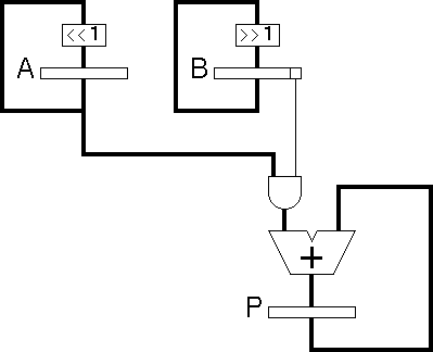
The simplest algorithm for multiplication involves repeated shift and add operations. In the figure below, the register A is initially loaded with the multiplicand and the register B is initially loaded with the multiplier while P which will contain the partial product is initially zero.
In the first cycle A is added to P if the least significant bit of B is '1'. A is shifted left while B is shifted right.
This process is repeated in subsequent cycles and completes when B=0. For a 4-bit multiplication the algorithm will complete in no more than 4 cycles.
The technique is simply one of long multiplication. Below you can see the long multiplication of two 4-bit values to produce an 8-bit result.
 Multiplicand         1011              11
 Multiplier           1101 x            13 x
                      ----             ---
                      1011              33
                     0000              11
                    1011               ---
                   1011                143
                  --------
 Product          10001111
The architecture shown above uses a 7-bit register for A and a 7-bit adder to produce an 8-bit result. This is an inefficient use of resources since we are never adding a value greater than four bits in length.
A more efficient implementation uses a 4-bit adder and four 4-bit registers:
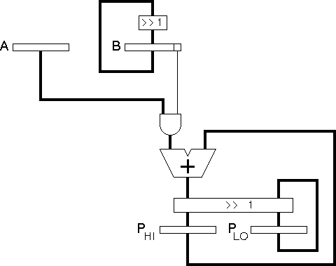
Note that PHI contains the four most significant bits of the partial product while PLO contains the four least significant bits.
The only disadvantage of this technique is that it takes 4 cycles regardless of the value of B (i.e. there is no opportunity to terminate the algorithm early where B is a small number).
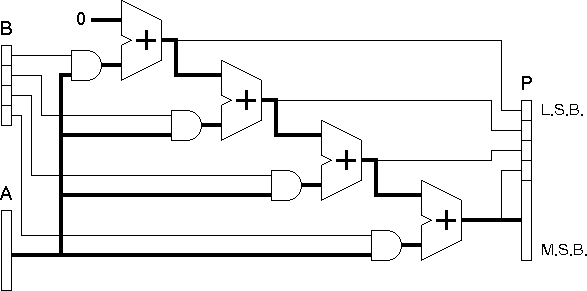
By replicating the hardware used in each cycle we can perform the multiplication within a single cycle.
More adders are needed and the clock cycle time must be extended but the overall time to produce each result will be slightly reduced (since the overhead involved in storing data between cycles is lost).
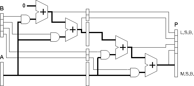
By adding pipeline registers we can increase the clock speed and hence the throughput while having a minimal impact on the latency.
In the system shown a single set of pipeline registers are added to provide a two stage pipeline. If the work done in each pipeline stage is well balanced we may expect to nearly double the throughput compared to the single cycle design.
The four designs presented so far show a range of different approaches to the problem. You could base your design on one of these or you could base it on another from the available literature or from your imagination. Should you base your design on one of these four you should be aware that they are not optimal (for instance the standard multi-cycle implemention saves on registers by using the same space for B and for PLO, while no single cycle or pipelined implementation should actually include an adder with one of its inputs held at zero).
Your final design choice should balance the requirements for performance against the limited resources you have available in terms of chip area and manpower. A simple design which fits and is submitted on time will always receive more marks than a potentially high performing design that is either too big to fabricate or submitted after the fabrication deadline.
The design must support the following inputs and outputs:
Inputs
This is a clock signal with an active rising edge. Thus all inputs may only be considered valid on the rising clock edge while the outputs should only change on the rising clock edge. This should be born in mind in particular if you choose to operate a two phase clocking system within your design.
This reset is asynchronous (independent of the clock) and active-low. Taking this signal low should reset your design to a known state.
This signal will go high for one clock cycle to indicate that a multiplication is required. Care must be taken to reject a second request while the resources of a multi-cycle multiplier unit are occupied with a multiplication. The ACK signal (see below) gives a method to indicate that a rejection has taken place. Holding this signal permanently high should result in multiplications one after another at the maximum speed permited by the design.
These are the four bits of the multiplicand. A3 is the most significant bit. The data will be presented at the same time as the STROBE signal. While the STROBE signal is low the data on these lines will be invalid.
These are the four bits of the multiplier. B3 is the most significant bit. The data will be presented at the same time as the STROBE signal. While the STROBE signal is low the data on these lines will be invalid.
Outputs
This signal indicates that a request for a multiplication has been accepted. It will go high for one cycle in the cycle following the the STROBE signal. On reset this signal will go low.
This signal indicates that the result is available on the Px outputs. It will go high for one cycle at the end of each multiplication. On reset this signal will go low.
These are the 8 bits of the final product. P7 is the most significant bit. The data will be presented at the same time as the READY signal. While the READY signal is low the data on these lines will be invalid.
Note that the signal names given here are case sensitive and are fixed. If you name your READY signal Ready or ready then the design will fail to simulate and will be rejected for fabrication.
As with any reasonably complex digital system you will need to divide and conquer when approaching the design. The first division that you should make is that between the datapath and the controller. The datapath includes the registers and functional units for manipulating the data, while the control unit will deal with STROBE, ACK and READY signals and provide any necessary control signals to the datapath (e.g. The alternative multi-cycle design would need a loadA signal to control the A register which is loaded at the start of the multiplication and thereafter must retain its value).
You are strongly encouraged to bitslice your datapath. A properly bitsliced datapath will result in a smaller and neater design. More importantly it will reduce the complexity of the place and route task by an order of magnitude thus increasing the chance of your design being submitted on time. You should end up with four identical bitslices each containing one quarter of the datapath. Because of the various shift functions inherent in the multiplication algorithm this division into bitslices is not trivial but is worth the effort.
Note that the first of the example designs uses a 7-bit adder and would therefore be better divided into seven bitslices. All of the remaining example designs use 4-bit adders and are suited to the four bitslice approach.
Iain McNally
14-2-2003