Integrated Circuit Engineering 2
The main features of the UoC Tiny Chip are:
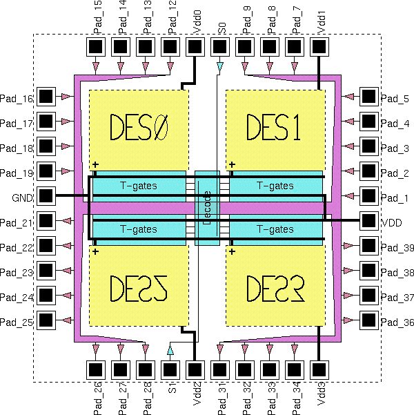
An outline of the frame is shown below:
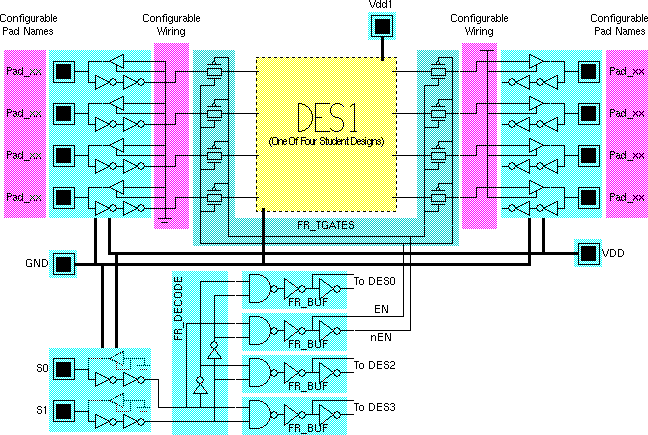
A more detailed view of the connections for one of the student designs is shown below:
When testing the DES1 design, S1:S0 will be set to "01" thereby disabling all transmission gates for the other three designs. Power will be supplied to the pad ring via VDD and to the DES1 core via Vdd1. All other core power pins (Vdd0 Vdd2 Vdd3) will be grounded. The result is that DES1 is isolated from the problems of other student designs on the same chip including port to port and even power to ground shorts.
This file contains flattened versions of pad cells from the MOSIS/Tanner supplied Hi-ESD pad library mamis050k.tdb. By flattening the cells we avoid a host of possible name conflicts when student designs are merged into the final frame.
The following pad cells are included:
PADGND PADVDD PADINC PADOUT PADAREF PADLESSCORNER
Note that the input and output pads (PADINC and PADOUT) are just customized versions of the bidirectional pad (PADBIDIRHE) which explains all the bidirectional pads in the figures above. Also note that the PADAREF cell is used for the core power pads (Vdd0 Vdd1 Vdd2 Vdd3) which provide power to the student designs.
This file contains the transmission gate and decode circuitry:
FR_TGATE FR_TGATES FR_BUF FR_DECODE
It also includes the user i/o pads with their configuration wiring.
FR_PADI FR_PADO
These are brought together with pads referenced from mAMIs05Pads.tdb and dummy designs (FR_DESIGN0 FR_DESIGN1 FR_DESIGN2 FR_DESIGN3) in an example frame:
FR_BASEFRAME
The last cell in this library is an uncustomized template for student designs:
FR_BASEDESIGN
This file is a technology file (containing no cells). It is used for importing a new frame from a GDS II file exported from magic should it be necessary to make any changes. This file defines mAMIs05Pads.tdb as a reference library.
This file is a technology file is used for final chip preparation. It references mAMIs05Frame.tdb which will in turn reference mAMIs05Pads.tdb.
This technology file includes more stringent DRC rules enforcing that contacts may not be stacked and that all objects are on a 0.5 lambda (0.15 micron) grid. These more stringent design rules were not included in other libraries for the 2003 exercise. They are now included in the example libraries (hopefully this will reduce problems during handin).
BIM_LIB.tdb contains the layouts and BIM_LIB.sdb contains the schematics and symbols for the example cells described in the Cell Library Documentation.
BIM_LIB.sdb contains cells named:
BIM_DFFR BIM_MSDR BIM_BUF BIM_CLKGEN BIM_LIBBIM_LIB.tdb contains cells named:
BIM1_DFFR BIM1_MSDR BIM1_BUF BIM1_CLKGEN BIM1_LIBwhich support over cell routing and
BIM2_DFFR BIM2_MSDR BIM2_BUF BIM2_CLKGEN BIM2_LIBwhich support routing channels which don't overlap with the cells.
These are the initial cell libraries provided to the students. The versions that currently exist include a template cell MY_DESIGN suitable for the 4 bit multiplier problem. The layout for MY_DESIGN includes a cell boundary and correctly placed and named ports. Within MY_DESIGN.sdb there is an empty schematic (ports only) for MY_DESIGN and also a complete symbol for the cell. Note that the complete symbol is required to support SLS simulation of schematics.
MY_DESIGN.sdb contains cells named:
BIM_DFFR BIM_MSDR BIM_BUF BIM_CLKGEN BIM_LIB MY_DESIGNMY_DESIGN.tdb contains cells named:
    BIM1_DFFR BIM1_MSDR BIM1_BUF BIM1_CLKGEN BIM1_LIB
    BIM2_DFFR BIM2_MSDR BIM2_BUF BIM2_CLKGEN BIM2_LIB MYDESIGN
All Tanner library files are in the TannerLibs directory which can be found at \\conada\courses\TannerLibs and which must be mounted as W:\TannerLibs for library and file referencing to work.
L-Edit
S-Edit
Support Files
Configuration is performed via the genUoCframe command acting on a specification file. Configuration may be considered as a two stage process (although both stages can be completed simultaneously). These stages are selection of pinout and selection of designs:
The task is to decide which pins on the final chip will be inputs and which will be outputs. In each case allocating a name to the chosen pin. Taking a very simple example in which the student task is to design a two input NAND gate, the following specification would suffice:
    pinout NAND
      1 Input A
      2 Input B
      3 Output Y
    end pinout
Here pins 1 and 2 are declared as inputs with names A and B, while
pin 3 is defined as an output named Y. The pinout as a whole is given
the name "NAND".
Remember when creating your own pinouts that the following pins are pre-defined: 6, 10, 11, 20, 29, 30, 35 & 40.
Assuming that this file where saved on Sun Unix machine as spec_ex1, the configuration is performed by typing:
genUoCframe < spec_ex1
The output from this configuration process is a device pinout file, NAND.dev which is used by the TesterGen software and the TestosterICs Functional Tester. If you examine this file you will see that unconfigured pins retain their default names (Pad_4, Pad_5, Pad_7 .. Pad_39) and are all defined as inputs.
In addition to this device pinout file, the pinout information should also be used to create a template design for the students. This template or base design contains the ports needed for connection of the student design into the frame:
Note that the unused ports (Pad_4, Pad_5, Pad_7 .. Pad_39) must exist on the final student design and must not be shorted to any other node since they will be connected to input pads in the frame.
A modified specification file, spec_ex2, will create a base design named MY_DESIGN with the correct pinout information:
    pinout NAND
      1 Input A
      2 Input B
      3 Output Y
    end pinout
    basedesign MY_DESIGN
Note that there must be no blank lines in the specification file since a blank line terminates the genUoCframe configuration script. Note also that the existing documentation tells the students that the base design will be called MY_DESIGN so it is probably best not to change this name. As before configuration is performed by typing:
genUoCframe < spec_ex2
The files created are NAND.dev (as before) plus MY_DESIGN.mag and MY_DESIGN.gds.
MY_DESIGN.mag is a magic file which can be viewed if you are running eXcursion in full 8-bit mode (i.e. the MS Windows display must be configured in 256 colour mode) using the command:
ex8magic7 MY_DESIGN
MY_DESIGN.gds is a GDS II format file exported from magic, suitable for import to L-Edit.
File -> Import Mask Data -> GDSII...
For the setup file use DRCTech.tdb. Other settings can be left as default.
GDS II can't cope with ports except as point labels so the cell boundary (which is a port on the Cell Outline Layer with name CELL_OUTLINE) must be added to the new L-Edit file. If the cell outline is drawn to surround the existing ports exactly, the lower right corner will be at {0.0, 0.0} and the upper left corner will be at {1432.0, 1278.0} where all coordinates are in lambda units.
If you copy the BIM1_LIB and the BIM2_LIB cells (with their hierarchies) you will automatically copy all the library cells.
In order to create the corresponding S-Edit file you will have to edit the MY_DESIGN cell in the existing MY_DESIGN.sdb file by hand. Remember to change the schematic and symbol views to suit the new pinout information.
Although example versions of these files are stored in W:\TannerLibs\mAMIs\EXLIBS2003\, New versions should be stored in W:\TannerLibs\mAMIs\ which is where existing documentation suggests that they will be found.
The task is to allocate student designs to their final locations on one or more chips to be fabricated.
Assuming that you have 7 teams AAA, BBB, CCC, DDD, EEE, FFF & GGG each team having provided a toplevel cell with a name of the form XXX_DESIGN (where XXX is their team identifier), you may allocate the first four teams to CHIP1. A new specification file, spec_ex3, will create a frame for CHIP1 which includes the designs as required:
    pinout NAND
      1 Input A
      2 Input B
      3 Output Y
    end pinout
    basedesign MY_DESIGN
    frame CHIP1
      0 AAA_DESIGN
      1 BBB_DESIGN
      2 CCC_DESIGN
      3 DDD_DESIGN
    end frame
The files created are NAND.dev, MY_DESIGN.mag, MY_DESIGN.gds (as before) plus CHIP1.mag and CHIP1.gds.
In each case the design will be correctly placed and correctly orientated (with CCC_DESIGN and DDD_DESIGN upside down) provided that the students haven't moved the ports. It would be good to develop a method for the students to check that they have not moved the ports or the bounding box for their designs as this would significantly reduce supervisor workload at handin time.
To complete the task we need to define a second chip, CHIP2, which includes the other 3 designs. In spec_ex4 below, we leave the DES3 position empty but it would also be possible to include a supervisor design in this space or to duplicate one of the student designs (maybe the best design from the other chip):
    pinout NAND
      1 Input A
      2 Input B
      3 Output Y
    end pinout
    basedesign MY_DESIGN
    frame CHIP1
      0 AAA_DESIGN
      1 BBB_DESIGN
      2 CCC_DESIGN
      3 DDD_DESIGN
    end frame
    frame CHIP2
      0 EEE_DESIGN
      1 FFF_DESIGN
      2 GGG_DESIGN
    end frame
The files created are NAND.dev, MY_DESIGN.mag, MY_DESIGN.gds, CHIP1.mag, CHIP1.gds, CHIP2.mag and CHIP2.gds.
File -> Import Mask Data -> GDSII...
For the setup file use mAMIs05ChipTech.tdb. Other settings can be left as default.
You will need to re-direct and then update the unlinked references for the student designs such that they point to appropriate versions.
For the 2003 exercise all designs were merged into a single ALL_DESIGN.tdb file before the import of the chip GDS II files. It was in this ALL_DESIGN.tdb file that the bounding box of each student design was checked.
Even though the bounding box may be correct, some students will probably have moved ports (by mistake or on purpose). Unless a better system is developed, the way to check this is to check alignment of the ports within the student design and the connections to the transmission gates by eye.
Some sort of a full simulation is necessary to gain confidence in the system. SLS should cope with a simulation of the full chip with four student designs. In the 2003 exercise it was possible to verify most of the designs in this manner but not all those that contained cascaded 6 transitor XOR gates (which cause problems for switch level simulators).
By default each chip will be saved in a new L-Edit file although it would be possible to subsequently merge all chips into a single file before fabrication if this was desired.
Iain McNally
9-6-2003