Quantum Nano-Electronics & Nano-Photonics
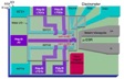
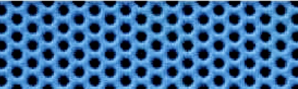
Graphene has rich physics based on the linear band structure with massless Dirac fermions. In the engineering points of views, graphne has significant potential for various nano device applications. The physical properties are rather exceptional in terms of band gap controls in nano structures, like graphene nano-ribbons. In the nano-ribbons, the band gap opening is observed depending on the patterned width of the ribbon. In our clean room, Southampton Nanofabrication Centre, we have a suitable tool to pattern it with in-situ characterization.
Grephene for nano devices
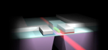
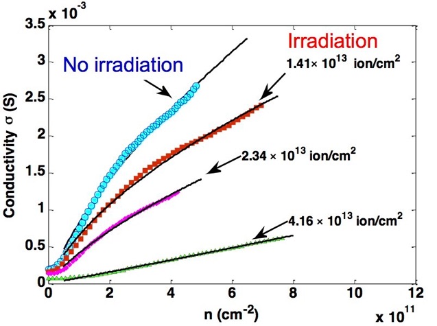
We have fabricated bilayer graphne field-effect-transistors to examine the transport characteristics for the scaled nano devices. We examined the conductivity dependence on the carrier density, and found that the diffusive scattering at the edge significantly reduces the conductivity. Moreover, we intentionally introduced the defects with the graphne by He ion bombardments, and found that the conductivity reduces accordingly. In this experiment, we confirmed that the scattering from defects is dominated over other scattering sources like phonons and ripples even at room temperature.
Graphne Field-Effect-Transistor
Transport Characterization
We have a lot to do for utilizing graphne in practical nano devices.
Collaborators:
Prof. H. Mizuta (Univ. of Southampton, JAIST)
Prof. H. Rutt, FREng (Univ. of Southampton)
Dr. Z. Moktadir (Univ. of Southampton)
Dr. S. Boden (Univ. of Southampton)
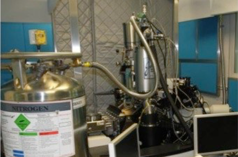
He-Ion-Microscope
Characterization & Patterning
beyond the conventional lithography limit.
Application of Massless Dirac Fermions
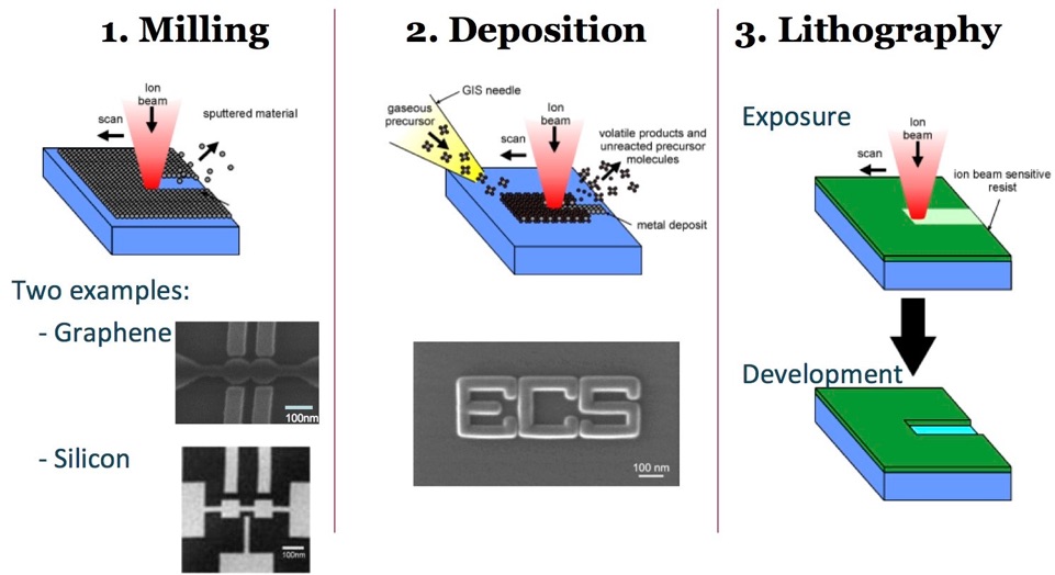
In the He-Ion-Microscope, the focussed He ion beams are used to take the image of the sample with a resolution, < 0.35 nm. In addition, we can mill thin films like graphene and Si quantum wells by increasing the power of the beam. We can also fabricate a complicated structure by using the combination of the resist patterning by He-Ion-Microscope and the conventional dry etching. We can fabricate the sub-5-nm minimum feature structures, which are beyond the current state-of-the-art Si technology in a fab.