CMOS Gate Array Design Exercise 2001-2002
You have been allocated 9 hours of laboratory time in which to test your CMOS Gate Array (CGA) designs. As a design team, the organization of your time is for the most part up to you. This document gives an outline of the tasks to be performed during this exercise and the available resources.
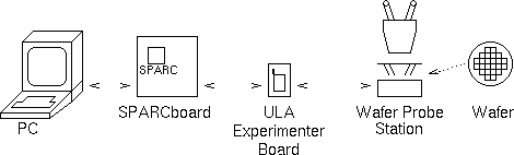
Before describing the tasks in more detail it is necessary to introduce the wafer testing equiptment.
Wafer Probe Station.
There are five Wafer Probe Stations in the electronics laboratory. These stations allow testing of chips prior to dicing and bonding. In this way we avoid wasting effort in packaging faulty chips.
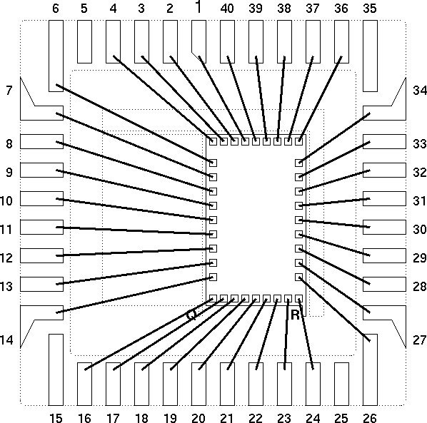
Each station should be fitted with a 36 pin probe card for making connections to CGA devices on a four inch silicon wafer. The probe card should be connected via ribbon cable to a 40 pin DIL header. The 40 pin DIL header is pin compatible with a bonded die.
The bonding diagram for 36 pin CGA devices in 40 pin DIL packages is shown below:
SPARC Board Computer.
The SPARC Board (or RISC Experimenter Board) acts as the main processor for this exercise. It is interfaced to the device under test via its on-board Peripheral Interface & Timer (PIT) chips and a dedicated ULA Experimenter Board. It communicates with you, the user, via an RS232 connection to a PC.
Each SPARC Board can run any of four EPROM based programs. By selecting EPROM image 4 and pressing Reset you can select the I.C. test software required for this exercise.
The SPARC Board should be connected via two ribbon cables to a ULA Experimenter Board. The 40 pin Zero Insertion Force socket on this board is designed to accept a CGA device in a 40 pin DIL package. It will also accept the 40 pin DIL header from the Wafer Probe Station.
Power is supplied to the device under test by an external power supply via the power connections on the ULA Experimenter Board. Connections are also supplied on this board for the monitoring of current drawn by the device under test.
PC.
The networked PC next to your SPARC Board acts as a terminal and file store. The machines should be linked via an RS232 cable from the COM2 port of the PC to SERA port of the SPARC Board.
The SPARC Board is accessed using the Windows Terminal Program set up for communication via COM2. Other parameters are; 19200 baud, 8 data bits, 1 stop bit, no parity and hardware flow control. This set-up is stored in a file called C:\WINNT\SPARC.TRM.
Test vectors can be stored on the PC and transfered between the PC and the SPARC Board using the Receive Text File and Send Text File facilities of the terminal program, or using Windows Cut and Paste facilities.
This circuit should use standard components and customized PLDs to mimic the behaviour of your CGA based Shaft Encoder Interface unit.
The circuit can be built on one or a number of Experimentor breadboards. For connection to other circuits, you should be supplied with a ribbon cable with 40 pin DIL headers at each end. The circuit should be pin compatible with the CGA version, including all testability inputs and outputs. Thus any system developed to test the CGA can be verified using the clone circuit.
hint - the most common mistake made by clone builders in the past has been to re-connect the testable blocks on the clone circuit boards - the result is a clone which no longer behaves like the CGA - a proper clone matches the functionality of the CGA exactly, including taking power from pins 14 and 34 and supporting a single RS flip-flop - think always is this exactly how the CGA version would behave?
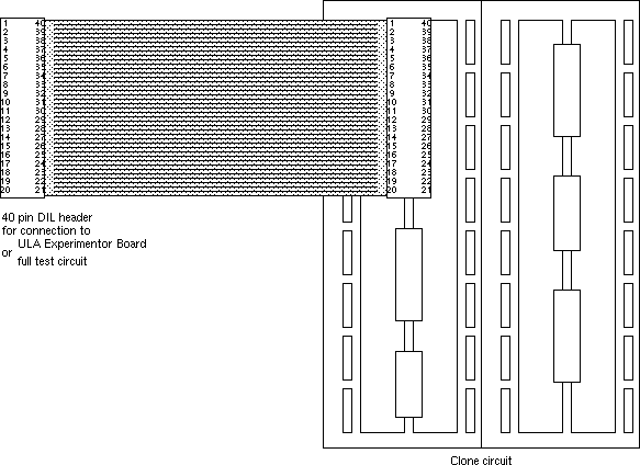
Where ISP PLD devices (e.g. ispGAL22V10) are used in the clone circuit, it is suggested that they are programmed out of circuit and then moved into circuit as required. It is possible to program the chips in situ but you need to be able to remove all the programming connections including power and ground in order to make use of the clone.
The SPARC Board computer allows you to create complex test vectors to check your circuit.
Test vectors are specified using a format statement followed by a number of vector specifications. The following test vectors might be used to check the RS flip-flop present on all chips:
  "Test vectors for RS flip-flop"

       "TESTnS TESTnR TESTQ"
    f     26     27     24

    v      0      0      H
    v      1      0      L
    v      1      1      L
    v      0      1      H
    v      1      1      H
    v      1      0      L
    v      1      1      L
The "......" indicates a comment that is ignored by the software.
The f command specifies the format of the test vectors in terms of pin numbers.
Each v command specifies a set of inputs {0,1,C,X} to apply to the inputs and a set of results {L,H,X} to expect on the outputs.
Using C as an input results in a 010 clock sequence on the pin. It is often useful to specify a number of clock pulses explicitly before using the C macro.
Using X as an expected output allows you to ignore the value of one output while you are testing another output. Although X is supported as an input, there is little benefit in using it since it is always interpreted as a 0.
You should aim to build up your test vectors until you have included tests for all parts of the circuit. The following vectors test the Next State cicuit from the simple simple sequencer example. Note that the f format command indicates a new set of vectors and will delete the existing vectors for the RS flip-flop. In order to perform both tests on a new site it is necessary to download and then run the RS vectors and then repeat the process for the Next State vectors.
  "Test vectors for the Next State circuit"

       "START  OUT_fn  Q1_fn  XOR     D0"
    f     31     32     33     37     36

    v      0      0      0      L      L
    v      0      0      1      H      H
    v      0      1      0      H      H
    v      0      1      1      L      L
    v      1      0      0      L      H
    v      1      0      1      H      H
    v      1      1      0      H      H
    v      1      1      1      L      H
Once you have debugged your vectors against the wafer you may like to combine sets of vectors to provide faster checking. In the following example, the first six vectors test the RS flip-flop, while the remaining eight test the Next State circuit:
  "Combined test vectors"

    f   26 27  24   31 32 33  37 36

        "Test vectors for RS flip-flop"

    v    0  0   H    0  0  0   X  X
    v    1  0   L    0  0  0   X  X
    v    1  1   L    0  0  0   X  X
    v    0  1   H    0  0  0   X  X
    v    1  1   H    0  0  0   X  X
    v    1  0   L    0  0  0   X  X

        "Test vectors for Next State circuit"

    v    0  0   X    0  0  0   L  L
    v    0  0   X    0  0  1   H  H
    v    0  0   X    0  1  0   H  H
    v    0  0   X    0  1  1   L  L
    v    0  0   X    1  0  0   L  H
    v    0  0   X    1  0  1   H  H
    v    0  0   X    1  1  0   H  H
    v    0  0   X    1  1  1   L  H
Remember - Only combine sets of test vectors after they have been checked as working against the wafer. This should avoid large amounts of wasted effort combining dodgy test vectors.
A number of vector manipulation commands are available while using the chip test software. Useful commands include:
Type help at the command prompt in order to see a summary of these and other commands.
Note that the chip test software is case sensitive. This means that the lower case "v" command used above differs from the upper case "V" command (which supports more formal, explicity numbered, vectors).
Note the importance of parallel development; the vectors can be used to debug the clone while the clone can be used to debug the vectors.
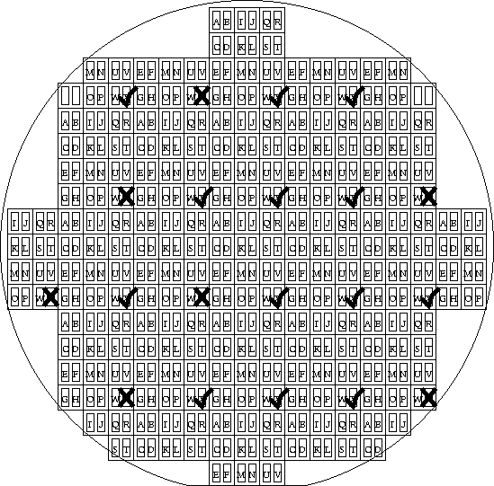
Each wafer has over 450 CGA sites, of which approximately 20 are yours. Having located your CGA sites, identified by the team letter below and to the right of each CGA site, you should test each site for random process failures and systematic design faults.
Where a systematic failure is observed (such as an output which never changes on any of your CGA sites or one which consistently exhibits strange behaviour), you should attempt to identify its cause. Most systematic failures are caused by errors at the design or implementation stages. In order to spot design errors, you will have to study your team's interim report and any netlist, icebox file or hard copy you have available for your design. Of course the most useful way to spot a design error is through simulation of your design.
Occasionally systematic errors can be caused during fabrication due to mask problems (since all 20 of your designs share the same stepper reticle masks). In this case you may find that changing to a wafer from a different batch will solve your problem. This is very rare, the majority of apparent systematic faults are caused by test vectors which don't match the design as you implemented it (either the design or the test vectors or both are in error).
In the event of a design error you may wish to modify your test vectors to test for the circuit as it was implemented, as distinct from as you had hoped it was implemented.
Where random process failures are observed, such as an output which works on one site but not on another, you should use your test vectors to isolate particular circuits which are in error. It is then possible to build up a map of these process failures for the whole wafer, showing where failures are more frequent and indicating where correct chips can be found. This map should contain as much information as time allows. It is usual to record static current consumption on such a map as it provides an extra indication of the health of a circuit.
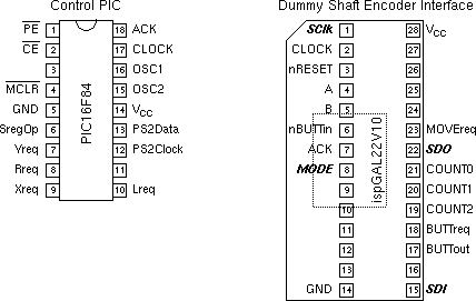
The full circuit shown in outline below includes:
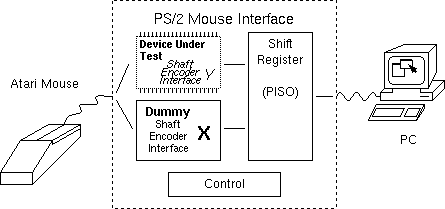
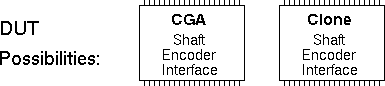
The circuit should expect a 40 pin DIL package containing the CGA Shaft Encoder Interface unit that you have designed (this is the DUT). During the design and implementation stages of this exercise you should have separated your Shaft Encoder Interface into a number of testable sub-circuits. These sub-circuits are re-connected here in order to create a fully functional PS/2 Mouse Interface.
This circuit can be fully debugged using the Shaft Encoder Interface clone in place of the CGA version.
The full circuit diagram is shown below:
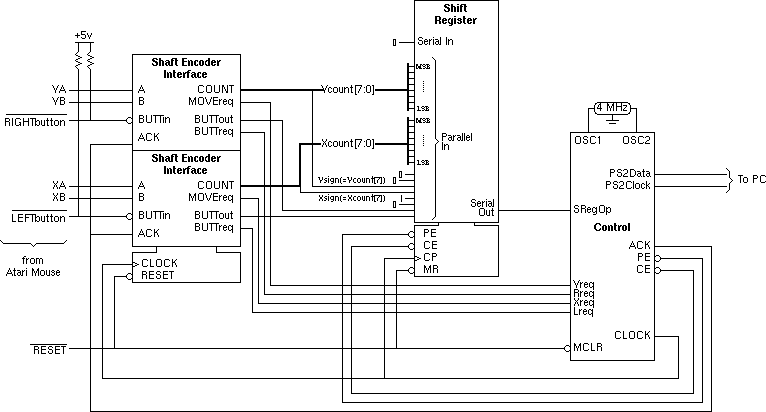
To simplify the task of building the full circuit, additional information is provided:
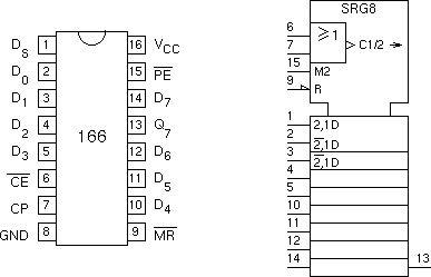
Once programmed, the pinouts for these two devices will be as shown below (note that where pins are not labelled they should be left unconnected):
| Start | Bit 0 | Bit 1 | Bit 2 | Bit 3 | Bit 4 | Bit 5 | Bit 6 | Bit 7 | Parity | Stop | |
|---|---|---|---|---|---|---|---|---|---|---|---|
| Byte 1 | 0 | Left Btn | Right Btn | 0 | 1 | X sign bit | Y sign bit | 0 | 0 | P | 1 |
| Byte 2 | 0 | X Movement | P | 1 | |||||||
| Byte 3 | 0 | Y Movement | P | 1 | |||||||
| Byte 4 | 0 | 0 | 1 | 1 | |||||||
The data for bytes 1-3 is provided from the 24 bit shift register while the control PIC is responsible for dealing with the Start, Stop and Parity bits. The control PIC is also responsible for generating the fourth data byte (=0) which would normally represent the distance travelled by the wheel.
Given this information about the protocol we can predict the output from the circuit. The following figure shows the output that you would expect from your circuit under a number of easy to reproduce conditions:
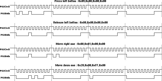
Check that you can follow these waveforms, identifying start, stop and parity bits. Note that data is transmitted least significant bit first and that the fourth byte is always zero since there is no wheel on our mouse.
When testing the full circuit you should ensure that you can reproduce these simple waveforms. Since these waveforms represent one-off events you will need to use a digital oscilloscope to capture them.
Check your waveforms before connecting your mouse to the PC. Connection to the PC will modify the waveforms seen, since the PS/2 connections are bi-directional. This check should also reduce the possibility of confusing the PC with corrupt data - thus avoiding time consuming reboot.
As with the test vectors you should use the clone to help in the debugging of your test circuit. A demonstration of the full system based on the clone is one of the deliverables for this exercise.
Having found a perfect CGA site (or one which is as near perfect as design and process failures allow) you should attempt to complete the exercise by connecting the CGA Shaft Encoder Interface to the full test circuit. You may need to bypass some CGA circuitry to make up for a less than perfect CGA sample.
In addition to the Wafer Probe Station, PCs and SPARC boards, you will need a number of items detailed below:
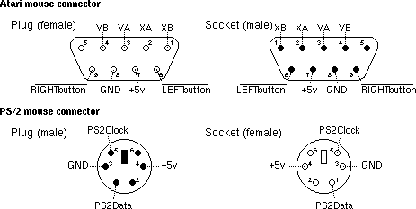
Note that you should follow the labels on the wires since their colours are neither consistent nor helpful (mine has a red wire for ground!).
Detail for mouse connectors:
The laboratory time is divided into two:
You should plan your work for the laboratory sessions and between laboratory sessions in order to make best use of the available resources.
In order to make most effective use of the wafers, you should attempt to get as much information as possible out of the wafer during the introductory session. Do not fall into the trap of performing simple tests over all of the sites on a wafer; having found one functional RS flip-flop you have demonstrated an absence of systematic faults in the flip-flop and checked your test vectors for the flip-flop. Move quickly on to tests for other simple sub-circuits.
This allows you to build clone and test circuits outside of the scheduled sessions.
In order to facilitate further testing, you may borrow these kits outside of your scheduled lab sessions provided that they are not required for other scheduled sessions and provided that you return them on the same morning/afternoon that you borrow them.
A small number of clone cables may also be available for you to borrow when interconnect kits are in use.
Iain McNally
11-4-2002