Integrated Circuit Engineering 2
| Week 1 | Monday 24th February | Assignment handed out |
| Week 3 | Friday 14th March, 5pm | Checkpoint 1 report due |
| Week 5 | Friday 28th March, 5pm | Checkpoint 2 report due |
| Week 9 | Monday 12th May, 2pm | Final design due |
| Week 10 | Monday 19th May, 2pm | Design report due (worth 20% of final mark) |
| Next Spring | Chips back from manufacture in USA | |
The object of this assignment is for you to design a CMOS circuit using full-custom design techniques. Once the designs are complete they will be fabricated (in the USA) using the MOSIS multi-project wafer service (www.mosis.org). They should be returned from fabrication in time for testing in the Spring.
"Principles of CMOS VLSI Design: A Systems Perspective", N. H. E. Weste, K. Eshraghian, 2nd Ed, Addison-Wesley, Reading Mass, 1993.
One of the cheapest ways to get your design to silicon is via a multi-project wafer. With this system various prototype chips are fabricated on a single wafer in order to share the costs (in particular the large NRE cost of mask production).
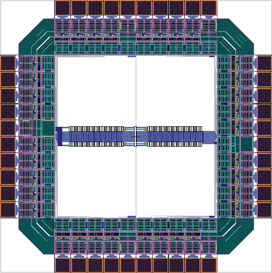
This project will use a multi-project chip on a multi-project wafer. Each design team will produce a full custom design to meet the specification provided. Four such designs will be included on each chip surrounded by a standard frame.
Four such chips will be sent to MOSIS (allowing for 14 student designs and 2 reference designs) where they will be fabricated on a single wafer along with designs from other universities and small companies.
With the full custom approach taken in this project, you must design and hand craft the leaf cells (basic gates) and then place and route them (again by hand) into a hierarchy of modules. This contrasts with a semi-custom approach in which you might typically make use of cells from a cell library designed by a silicon foundry and then use automated place and route tools to convert a circuit schematic or hardware description language model into the final design. The full custom approach gives you more control over the design parameters and, if designed well, the resultant circuit should be smaller and/or faster than an equivalent semi-custom design. Even where your design doesn't outperform a semi-custom design, the full custom approach will give you much better insight into the IC design process and is hence preferred for educational reasons.
A detailed specification for the circuit that you must design is included within the specification document.
The assignment has been broken down into four sections.
In practice, large teams of engineers design VLSI chips. Although you will be working on a small design, the amount of work involved is quite large. Therefore you will work in twos or threes. Two is the preferred group size.
Your layout will be completed to meet the specification of one of the MOSIS processes. MOSIS are based at the University of Southern California and act as a convenient interface between universities and several major chip manufacturers. Your designs will be made using AMI's 0.5 µm N-well process. You will need to learn the details of the process to ensure successful design. The process parameters will be imported automatically with the start-up file (see later in this document). A full description is available from MOSIS at www.mosis.org/Technical/Designrules/scmos/scmos-main.html . Weste and Eshraghian also contains most of the information.
The process properties are for SCN3MSUBM:
Tanner Tools, Tanner Research Ltd.
This version of the widely used PC based layout editor includes facilities for design rule checking and circuit extraction for Spice simulation.
This Spice tool integrates well with the other Tanner tools and should be your first choice for analogue simulation of L-Edit designs.
This is a basic schematic editor using a user interface similar to that of L-Edit. It can be a valuable tool to improve your productivity since mistakes made at the schematic stage can be corrected much faster than mistakes in layout.
Note that this year all Tanner tools are available on all CAE-2 PCs.
Space Tools, Delft University of Technology
Space circuit extraction is more sophisticated than L-Edit extraction and can provide netlist files for both digital and accurate analogue simulation.
Although analogue circuit simulation may yield timing information, simulation times may be excessively long for large designs. In contrast, digital switch level simulation will provide near instantaneous results for the sort of design that you are building and is essential to verify the functionality of the final system.
All Space tools run on Sun Unix machines but may be accessed remotely via Windows PCs.
You may also find yourself using Berkeley Spice software in conjunction with the more accurate Space analogue circuit extraction (since Berkeley Spice runs on the Sun Unix machines).
This assignment is worth 20% of the total assessment for ICE 2. The main submission will be a written report produced by each individual and submitted in Week 9 along with your design data. This report will determine the majority of your grade for the assignment. In addition to this, each group will submit brief reports (a few pages of results) at a number of checkpoints during the assignment (prior to the main report submission). The purpose of these reports being to make sure that you will be able to meet the STRICT deadline for submitting your design. Submission of the checkpoint reports is compulsory, and a 5% penalty will be imposed on your main report grade for each checkpoint report not submitted on time (although the checkpoint reports will not carry any weight for your final mark so long as they are satisfactorily submitted).
Naming conventions are essential when handling large amounts of design data. Normally one uses a convention or code that uniquely and meaningfully identifies the function of a cell. e.g. AB_C defines a cell with the boolean function F = AB + C. In the present case we have a somewhat different problem. Each team will be designing a similar circuit that will be fabricated on a single chip. In order to discriminate between the designs, each of you MUST ensure that your file name is not duplicated. Furthermore, you MUST ensure that your cell names are not duplicated since all the cells will be incorporated into one big file for fabrication. For example, we do not want to end up with ten NAND2 gates, all with the same name, since data will be lost. To eliminate these difficulties you MUST USE the following naming convention. NB: A log of all the group personnel and naming convention each group uses will be recorded at the beginning of the exercise to ensure that no coincidences occur.
File name
Your file name will consist of no more than eight characters. The first pair of letters will be the first and last name initials of one of the team. The second pair of letters will be the initials of another team member, and the same for a third. Each pair of initials may be delimited by an underscore. The file extension will be ".tdb" (Tanner DataBase). Example: a team made up of Richard Blaikie and Rebecca Cheung would use the file name "RB_RC.tdb".
Cell names
The first few characters will be your team initials as before. The remaining characters should identify the cell function. E.g. if Richard Blaikie and Rebecca Cheung were to design a XOR gate then the cell would be called "RBRC_XOR". (Note: do not exceed 12 characters.) Failure to comply with these rules could lead to severe difficulties.
Common sense
In the event that two teams share the same initials, be sensible and don't use them in the same order. If you are a threesome, use a sensible shortening of the six initials available for cell naming. Above all, be consistent!
When you reach the stage that you are ready to begin layout you should copy the file W:\TannerLibs\mAMIs\MY_DESIGN.tdb into your user space. Rename the file so that it is identifiably yours (refer to the naming conventions in the last section).
This file includes an initial library of cells which you can use as the basis for your own cell library. All of these cells have names beginning with BIM1_ or BIM2_. Even if you use these cells unmodified you should rename them according to the naming conventions in order to avoid naming conflicts when designs are merged.
These cells are discussed in more detail in the cell library documentation.
In addition this file includes a cell called MY_DESIGN which defines the space into which your design MUST fit. If you like, this is your piece of chip real estate that will fit into the multiproject chip's floorplan. DO NOT STRAY OUTSIDE this box with your design. If you do, your design WILL NOT go to fab.
If you inspect MY_DESIGN closely you will find several labelled ports laid out in metal 1, 2 or 3. In addition to fitting inside the space defined by MY_DESIGN, your design MUST make electrical connections on the appropriate metal layer to these ports with the correct signal. If you do not satisfy this requirement, then your design WILL NOT go to fab.
The names and functions of these ports are discussed further within the specification document.
Important
Before handin, your design will have to be placed inside your version of the cell MY_DESIGN (this cell also will have to be renamed according to the naming conventions). Do not start by building your design within this cell, the chances of you corrupting it are very high. Instead build your design within a core cell sized to fit within this cell and then instance the core cell within your version of MY_DESIGN when you are ready for final simulation and design submission.
Based on the design specification your task is to create a top down design (first an outline architecture and then more detailed designs of modules) finishing with gate-level schematic diagrams. You should aim to keep the number of gates and the number of types of gates used in these gate-level schematics to a minimum.
Remember to keep your design simple so that you increase your chance of completing on time.
Each group should prepare a short document (approx 4 pages) describing the data path architecture (including a block level schematic) and detail of the gate-level design for the modules to be constructed (e.g. gate-level schematics of the control unit and of one bit of the bitsliced datapath).
List and make clear what leaf cells you need to design. Also state which cells from the initial cell library you will be using.
These progress reports are to be handed in (one submission per team).
Having identified all the leaf cells you must now design them.
Leaf cells should use M1 (metal 1) for power rails M2 for signal inputs and outputs. If leaf cells are designed without the use of M2 or M3 for internal routing then the cell is suitable for over-cell routing using M2 vertically and M3 horizontally. The example cells in the initial cell library have been designed in this style. If M2 or M3 is used within the cell then input/output should be at the top and bottom of the cell in a manner suitable for non-overlapping routing channels. Note when using multiple metal layers that contacts should not be stacked (although the DRC does not pick this up). Thus via should not be placed on top of poly/active contact and via2 should not be placed on top of via (via2 over poly/active contact is not a problem).
In an ideal full-custom design every transistor in every gate can be independently optimized to give the best overall circuit performance. With the size and complexity of this design you will have to make compromises to produce individual leaf cells which may be used in a number of different locations within the circuit. Decisions on transistor sizing should be affected by requirements for
Each cell that you design should be simulated using T-Spice. For completeness you should also simulate any cells from the initial cell library that you chose to use.
When using the L-Edit circuit extractor you will need to use the correct extraction file which is W:\TannerLibs\mAMIs\mAMIs05.ext. For your simulations you should ensure that your netlist contains the line
.include W:\TannerLibs\mAMIs\mAMIs05.md
This ensures that you are using the correct device parameters. The extraction tool should get these right if you start with provided start-up file.
For these simulations you should set VDD = 5V since the frame contains I/O pads designed for this voltage.
When you perform your simulations you should extract the propagation delay for both rising and falling edges for the load conditions described below. For your chosen D-Type (either edge triggered or master slave) you should extract the setup and hold times and the clock to Q delay. Ideally you should do this for capturing both a 0 and a 1.
For each cell you should simulate with a load equivalent to a unit inverter and then with a load equivalent to two unit inverters (the unit inverter for the initial cell library is nominally set with Wn=17lambda and Wp=34lambda). From this you can get a nominal delay for one inverter and a delta delay indicating the effect if the loading is increased. This should be enough to predict any delay with reasonable accuracy provided that you know the loading at any node (expressed as gate equivalent load based on the unit inverter). Hence the next task for each cell is to calculate a value for gate equivalent loading at each input.
When your design is complete you should simulate it in its entirety. In the meantime, take a short cut. Using the timing data from all your leaf-cell simulations, estimate the propagation delay for the critical path through the combinational logic, hence the maximum frequency of operation. Remember to factor in the setup time and clock to Q delay of your chosen D-Type.
Note that this is probably the appropriate time to consider adding buffering to your design where you find the relative fan-out at a node is too large.
After completing this work you should submit short data sheets for each of the leaf-cells, including any cells you use from the initial cell library. These data sheets should occupy about half a page of A4 each and contain a truth table and the timing and loading information that you have extracted. You should also append a transistor level schematic diagram, layout, netlist and ONE graph from simulation for each cell and give an estimated maximum clock speed for the complete system. (One submission per team.)
Once you have assembled all the leaf cells you should then build up the required modules to complete the design.
Within each module the cells should be placed in rows in order to create the required VDD and GND connections between cells. Next critical signals e.g. clock(s) and common signals e.g. reset should be routed using two level routing in keeping with the choices you have made for your cell library (e.g. M2 vertically and M3 horizontally with no routing over leaf cells). Finally the remaining signals are routed using two level routing to complete the module.
Note that if your cell library is designed for over cell routing, you should be careful not to overlay an M1 M2 contact (via) within the leaf cell with an M2 M3 contact (via2) in the routing since this will create a stacked contact.
When you get to the placement of sub-modules to produce the next level up in the hierarchy, it is strongly suggested that you do not allow routing over the sub-modules. If input/output signals are be available at the edge of the sub-modules this sort of routing can be safely avoided. The reason for this restriction is that the process has insufficient metal layers to do this safely (ideally over module routing would be done in M4 and M5 which aren't included in this process).
Proper consideration of clock buffering and distribution is essential at this stage in order to avoid clock skew and associated race hazards. Depending on the size of the modules you might choose to include a level of clock buffering within the top level module to perform the distibution to sub-modules and further buffering within the sub-modules to distribute the clock to the D-Types.
Your complete design MUST fit into your space allocation. This is bounded by the region defined in the cell MY_DESIGN in the startup file.
In order to do this you must indicate which cell is the top-level cell using the L-Edit command "Fabricate" in the Cell menu. Once you have done this, e-mail the ".tdb" file to I.McNally@elec.canterbury.ac.nz as an attachment with the name of the top cell clearly stated. You should also submit a printout of your top cell to facilitate the error checking procedure.
More information can be found in the web document E-Mail File Submission.
The CHECKPOINT reports you will have submitted already are mainly intended to track your progress with the assignment and find any major difficulties/errors before it is too late. With the expense of going to fab, we don't want to take any chances. However, they will also be a part of your assessment and you can reuse the material (with appropriate description) in you final report. The report must describe what you have done, why you have done it, and present all your results. A concluding discussion about your design, how (if at all) you would improve it and other issues is expected (not merely a technical report of what you did). Each member of every team must submit a separate report. All team members can submit material reused from CHECKPOINT reports.
Remember to acknowledge your sources, e.g. system designs derived from Wakerly or circuit designs and layouts taken from Weste & Eshraghian. Also acknowledge any designs taken from the initial cell library whether or not it is modified. Since this is a team effort, you should be sure to acknowledge the work from other team members and if applicable the work of other students from other teams.
The Design Report is not to exceed 30 pages in length.
Iain McNally
22-2-2003