About the Characterisation facilities
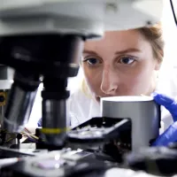
We host a range of equipment that can be used for device and material characterisation.
We provide high resolution imaging of different types of specimens ranging from biological to semiconductor materials:
- plan view imaging of a sample surface using field emission scanning microscopy (FESEM), helium ion microscopy or scanning probe microscopy (SPM)
- cross-section imaging using the focussed ion beam (FIB) system and FESEM
- imaging of biological samples in liquids using an environmental scanning electron microscope (SEM)
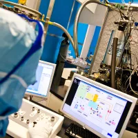
We also have tools for preparing, measuring and analysing specimens. This includes:
- preparation of thin samples for transmission electron microscopy using the FIB system
- depth profiling of material composition using secondary ion mass spectroscopy (SIMS)
- analysis of sample composition using X-ray fluorescence and X-ray computed technology
- measurement of film thickness using ellipsometry
- measurement of step heights after etching using spectroscopy
- electrical and RF testing.
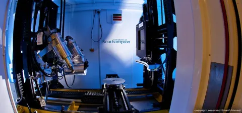
Our characterisation facilities are part of the clean room at the nanofabrication centre.