
Etching facility

More Information

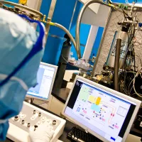
About the Etching facility

Etching is a key fabrication process for pattern transfer after lithography. We have both dry etching  and wet etching systems which can be used in:

  • silicon processing
  • metal etching
  • dielectric machining
  • thin film processing
  • semiconductor materials (type II, III, V, and N).

Wet etching

Wet etching provides a simple and cheap method of pattern transfer, but gives little control over the etch profile. We offer wet etches and cleans including:

  • hydrofluoric acid for oxide etching
  • fuming nitric acid for resist strip
  • RCA clean for wafer cleaning prior to furnace or rapid thermal processing.

Dry etching

Dry etching allows the etch profile to be varied from anisotropic to isotropic. The etch chemistry is much more complex. High resolution pattern transfer is done through reactive gas chemistry and plasma etch technology. We offer these types of dry etching technologies:

  • reactive ion etching (RIE) for general etching such as silicon (amorphous, poly), silica, silicon nitride, polymer, metal and resist residue cleaning, metal etching and for III-V semiconductor materials. 
  • deep reactive ion etching (DRIE) for silicon-based MEMS and NEMS devices where anisotropic profiles are essential
  • inductively coupled plasma etching (ICP) for metal-contaminated and metal-free processes
  • ion beam etching (IBE) for hard materials such as Si, Ge, GaN, sapphire and metals

The etching capabilities are part of our clean rooms at the nanofabrication centre.

Technical specification

Wet etch room

The wet etch room provides a safe environment for wet etch and cleaning processes. We have:

  • dedicated wet benches for etching and stripping various materials
  • acid tanks for process cassettes of substrates sizing from 50 to 200 mm
  • KOH and TMAH tanks for wet etching of silicon
  • wet benches can also be set up for electroplating processes

We have also established a set of wet chemical processes:

  • 7:1 buffered hydrofluoric acid for thermal oxide etch
  • 20:1 buffered hydrofluoric acid for thermal oxide etch
  • orthophosphoric acid at 160C for silicon nitrate etch
  • orthophosphoric acid at 37C for aluminium etch
  • potassium hydroxide at 70C for silicon anisotropic etch
  • RCA clean for wafer clean
  • fuming nitric acid for resist strip and wafer clean

DRIE

Our DRIE system uses advanced silicon etch (ASE) technology, based on the Bosch process, to achieve rapid and very deep silicon etch profiles with a smooth sidewall. The system offers:

  • accepts smaller samples up to 200mm wafer
  • SF6/C4F8/Ar/O2 gases
  • etch rates typically of >2um/min at 5um and >7um/min at 80um
  • 90+1°, 20nm rms sidewall roughness
  • aspect ratio - PR>30:1, SiO2>60:1

RIE

We have three RIE systems that are distinguished by the available gases and metal or metal-free substrates processing:

  • two Plasmalab 80 plus (I) systems which are fluorine-based chemistry etching tools, alternatively argon and oxygen
  • Plasmalab 80 plus (II) system which is a chlorine-based chemistry etching for metal etching and suitable for III-V semiconductor materials

ICP

We have two ICP systems dedicated for metal-contaminated and metal-free processes:

  • Plasmalb system 100 which is a dielectric and Si etcher offering fluorine-based chemistry etching
  • Plasmalab System 100 for metal, dielectrics and Si etcher offering chlorine/bromine-based chemistry etching

IBE

Our IBE system is an Ionfab 300 plus configured for MEMS and NEMS structures, silicon-based material, silica, quartz and deep etch structures. The system has the following capabilities:

  • can take up to 200 mm wafers
  • substrates can be tilted to perform angular etch

Surface decontamination systems

We also have several surface decontamination systems:

  • UV ozone cleaner used for remove surface contaminants, UV curing, improving surface hydrophobicity and oxidising surface of substrates.
  • oxygen plasma etching systems used for stripping resists and de-scumming substrates.

Etching facility

Contact us

Contact us

Mountbatten Complex, School of Electronics and Computer Science, University of Southampton, SO17 1BJ
Back
to top