
Chemical nanoanalysis scanning electron microscope

More Information

About the Chemical nanoanalysis scanning electron microscope

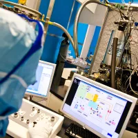
The Chemical Nanoanalysis Scanning Electron Microscope (CNSEM) facility offers a high resolution field emission SEM, in combination with dual-EDS and correlative Raman spectrometer.

The first EDS detector is suitable for elemental composition analysis, typically between 5 – 30 kV at high throughput mapping.

The second EDS is windowless with element detection down to Li Ka (56 eV) and intended for low energy work <5 keV for superior surface sensitivity.

For the Raman analysis the sample is translated over to a 100x objective lens within the chamber, where the laser spot size is ~360nm, offering sub-micron mapping capability. Raman offers complimentary chemical information to EDS, allowing you to fingerprint polymers, and ordered and disordered structures.

Highlights

  • imaging resolution down 1 nm - InLensDuo for improved surface sensitive imaging
  • Oxford Instruments Ultim 170 EDS
  • Oxford Instruments Extreme 100 EDS
  • WITec Raman RISE
  • sample shuttle for air-sensitive sample mounting inside a glovebox
  • plasma cleaner

Technical specification

Zeiss Sigma 500 VP FESEM

  • Field Emission Source - 20 nA configuration
  • Resolution: 0.8nm at 15 kV, 1.4nm at 1 kV
  • Variable Pressure (VP) using N2 (10 – 133 Pa) : 1.5nm at 30 kV (for uncoated non-conductive samples)
  • Imaging Detectors:
    • SE2
    • AsB
    • InLensDuo SE & BSE (energy selective)
    • C2D for VP mode
  • 80mm Air-lock for sample transfer XEI Evactron E50 Plasma Cleaner
  • SemiLab air-sensitive sample shuttle (for loading samples inside a glovebox and opening remotely once inside SEM)

Oxford Instruments EDS

  • Ultim X-Max 170mm2
  • Ultim Extreme 100mm2 windowless
  • Sub 10nm mapping possible
  • Aztek Advanced Software
  • LayerProbe for thin film analysis (layer thickness and composition correction)

WITec Raman RISE

  • 532nm laser diode / 32 mW
  • 100x objective 0.75 NA
  • 600 & 1800 grating
  • scanning/mapping done by piezo-stage objective
  • acquisition modes: point spectrum, line scan, mapping (area, depth and 3D)
  • data processing with Project Five Plus
Back
to top