About the nanofabrication cleanrooms
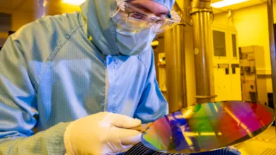
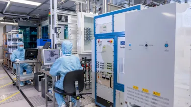
The Southampton Nanofabrication Centre (SNC) houses a fully featured suite of semiconductor processing tools up to 200 millimetre (mm) wafer scale. The Integrated Photonics Cleanroom (IPC) is a planar fabrication laboratory using a more diverse spectrum of materials compared to a standard SEMI fab.
Our dedicated engineers and technicians respond to both research and industrial needs. We manage all aspects of process development, integration and customisation for application-specific requirements.
We can also train your staff to operate tools within the cleanrooms.
Our flexibility allows us to process from 200mm wafers to diced samples, with device dimensions from hundreds of micrometres (µm) to under 10 nanometres (nm).
We have expertise in processing a wide range of substrate materials, for example:
- Si (silicon)
- SiO2 (quartz, fused silica)
- SOI (silicon on insulator)
- Ge (germanium)
- SiGe (silicon germanium)
- III-V (3-5 compound semiconductors)
- SiC (silicon carbide)
- sapphire
- glass/pyrex
and can use a broad range of additive materials:
- metals
- dielectrics
- semiconductors
- chalcogenides
- polymers
- organics
We can setup virtual lines for dedicated applications and pilot production activities.
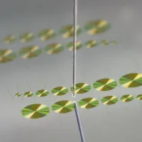
Additionally, we offer a silicon photonics multi-project-wafer (MPW) service via our CORNERSTONE programme. This is part of the EUROPRACTICE initiative, which lowers barriers for manufacturing smart integrated systems and electronic circuits. It serves both industry and academia.
Virtual tour
Explore our state-of-the-art facilities — take a virtual tour of Southampton nanofabrication cleanrooms and integrated photonics cleanroom.

