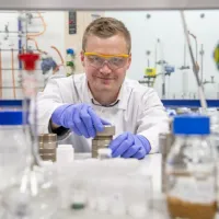
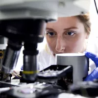
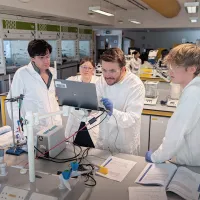
Material innovation laboratory

More Information

About the Material innovation laboratory

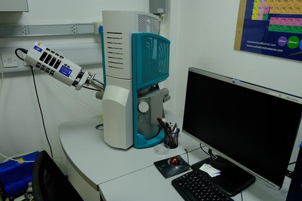
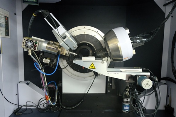
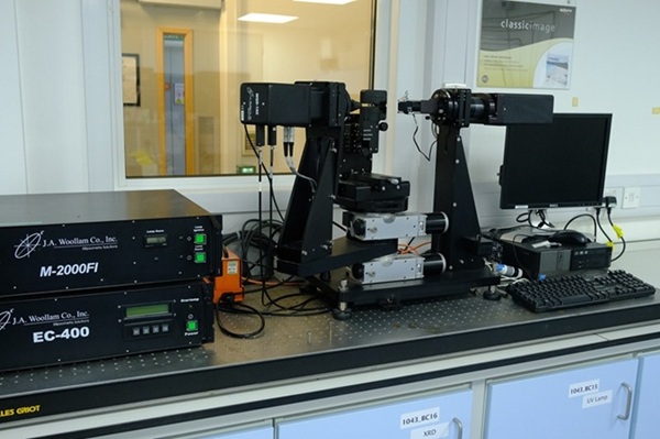
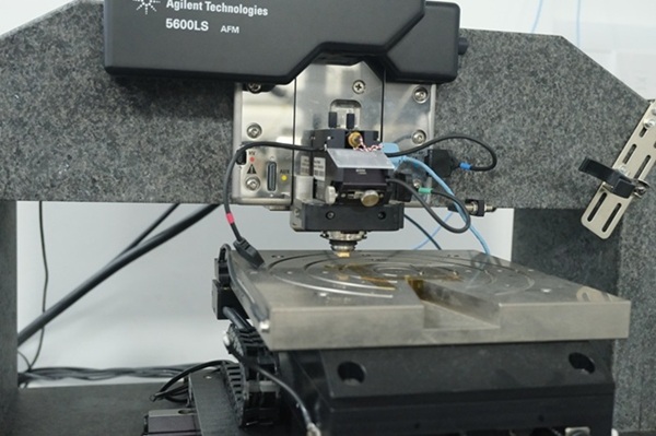
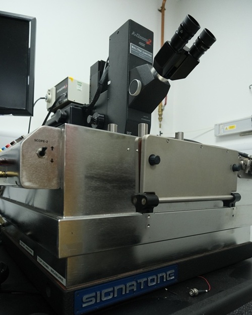
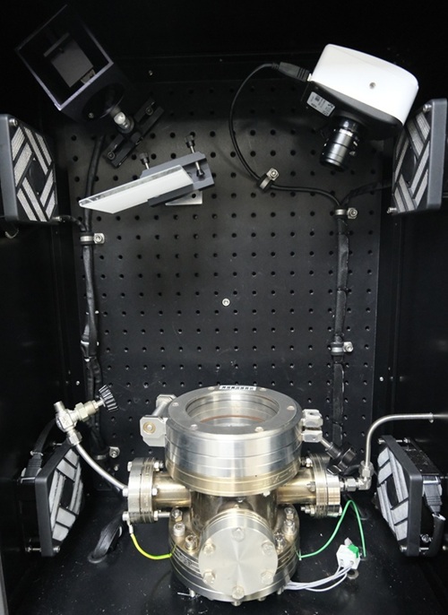
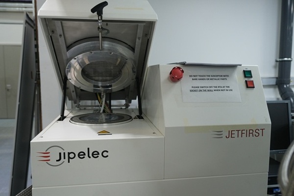
Material research projects, thin film synthesis and thin film characterisation

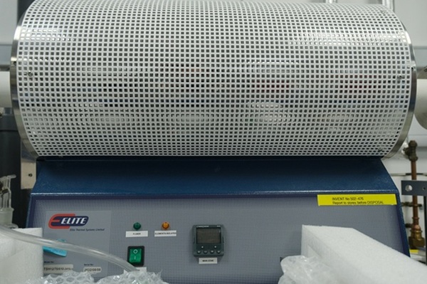
The material innovation laboratory facility offers a range of capabilities ranging from synthesis and characterisation to full research projects focusing on high-throughput methodology

The technology and setup available at the facility allow us to rapidly explore the compositional dependence, for a given family of materials, of chosen and specific fundamental characteristics.

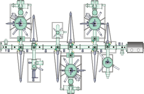
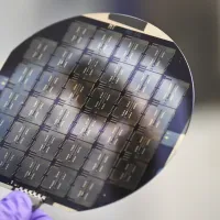
High-throughput synthesis of thin film samples is combined with automated characterisation to efficiently acquire a unique and complete dataset of the material family. Using tailored software, the data is combined and analysed to produce an understanding of the relationship between composition, crystal structure and selected physical properties.

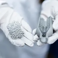
This approach has been implemented to study phase change memory materials, advanced alloys, functional ceramics, dielectrics, metals, electrocatalysts, battery materials (anodes, cathodes and electrolytes), hydrogen storage materials, gas sensors, thermoelectrics and photovoltaics as well as optical coatings and plasmonic materials.

The facility operates as an Engineering and Physical Sciences Research Council (EPSRC) small research facility and can be included on grant applications.

It also offers a contract service for external users upon discussion with the facility manager via the nC2 Engineering Consultancy.


Three logos of the Material Innovation Laboratory, combining the logo of the university of Southampton with the words Milab and Material Innovation Laboratory in Green and blue

Technical specification

High-Throughput evaporative Physical Vapour Deposition (HTePVD)

  • modified molecular beam epitaxy (MBE) system based on 100 mm wafer

    • 3 x M600 chambers for up to 6 evaporation sources and one radio frequency (RF) atom source
    • co-evaporation of up to 6 elements possible
    • rotating heated manipulators up to 900 °C
    • synthesis of material libraries on 35 x 35 mm substrates

  • 6 x 3” targets radio frequency (RF) and direct current (DC) sputterer

    • simultaneous deposition of up to 2 target materials
    • argon or reactive sputtering
    • rotating, heated manipulator

  • in vacuum x-ray photoelectron spectroscopy (XPS) system with automated X-Y stage
  • two high vacuum (HV) Load Locks, one with integrated glove box for sample preparation/protection
  • sample manipulation under ultra high vacuum (UHV) environment
  • sample storage and contact mask transfer capability in UHV
  • annealing chamber under vacuum up to 1100 °C
Complex mechanical apparatus with multiple cylindrical components attached symmetrically on either side.


Automated characterisation

PropertyTechniqueArray sizeAcq. Time
CompositionEDS14x144h
StructureXRD14x1412h
Temperature induced changesHTOMPT14x14 (cont.)6h
Optical constantsEllipsometry14x143h
Electrical resistance4PP14x142h-12h
Electrical impedanceLCR meter14x146h
Electrochemical reactionselectrochemistry10x10 
CompositionXPS5x54h


SEM-EDS

  • TESCAN VEGA scanning electron microscope equipped with Oxford Instrument energy dispersive spectroscopy detector (SEM-EDS)
  • secondary electron imaging (SEI) and backscattered electron imaging (BSE)
  • INCA and AZTEC software
A laboratory desk setup with an electron microscope and a computer monitor.


X-ray diffraction

  • Bruker D8 platform
  • Incoatec microsource, copper (Cu) radiation, 0.5 mm diameter
  • 2D general area detector diffraction system (GADDS)
  • large, motorised X-Y-Z stage movement
scientific instrument, likely an X-ray diffractometer, within a laboratory setting. At the center is a circular component with a black and white design, flanked by mechanical arms and electronic attachments.


Ellipsometer

laboratory setup featuring a sophisticated piece of equipment resting on a perforated metal table. Central to the setup is a black electronic device consisting of two vertical supports connected by a series of horizontal platforms and components, likely used for scientific measurement or research.


Atomic force microscope

  • Agilent 5600LS AFM

a precision scientific instrument setup, likely an Atomic Force Microscope (AFM). The main body of the microscope has a dark upper section. Below it is a metallic panel with embedded screws, wires, and technological components.


Probe station

  • signatone Probestation to enable automated electrical characterisation of materials

    • HP4284A – Precision LCR meter – 20Hz to 1MHz, ± 20 Vdc bias
    • network analyser
    • semiconductor device analyser
    • Keithleys DC SourceMeters and MultiMeters
    • ferroelectric tester
Piece of laboratory equipment, specifically a microscope setup with dual eyepieces mounted on a metallic platform and placed in a lab environment. The equipment features several knobs and controls.


HTOMPT (High-throughput optical mapping of phase transitions)

A metallic cylindrical device with a transparent window on a perforated panel, surrounded by cameras and connectors.


RTA (Rapid thermal annealer)

  • Jipelec 150 RTA
  • 150 mm wafers max
  • up to 1200 °C
  • controlled atmosphere
A laboratory machine with an open chamber, branded as "Jipelec" and "JETFIRST," showing its metallic interior and featuring an emergency stop button. The top section of the machine is open, revealing a circular metallic part with a glass section at the centre.


Tube furnace

  • 100 mm diameter tube furnace
  • controlled atmosphere
A cylindrical laboratory furnace with a metal mesh cover on a blue control unit with labelled buttons.

Contact us

Contact us

For more information get in touch.
B27 Room 1057, School of Chemistry and Chemical Engineering, University of Southampton, Southampton, SO17 1BJ
Mon-Fri 10 am – 4 pm

Follow on social media