Skip to main content
Study
Student life
Research
Our impact
Research projects
Research areas
Research facilities
Collaborate with us
Institutes, centres and groups
Active Living
Advanced Fibre Applications
Advanced Laser Laboratory
Advanced Project Management Research Centre
Antibody and Vaccine Group
Astronomy Group
Autism Community Research Network @ Southampton (ACoRNS)
Bioarchaeology and Osteoarchaeology at Southampton (BOS)
Bladder and Bowel Management
Cell and Developmental Biology
Centre for Defence and Security Research
Centre for Developmental Origins of Health and Disease
Centre for Digital Finance
Centre for Eastern European and Eurasian Studies (CEEES)
Centre for Empirical Research in Finance and Banking (CERFIB)
Centre for Geometry, Topology, and Applications
Centre for Global Health and Policy (GHaP)
Centre for Green Maritime Innovation (cGMI)
Centre for Health Technologies
Centre for Healthcare Analytics
Centre for Human Development, Stem Cells and Regeneration
Centre for Imperial and Postcolonial Studies
Centre for Inclusive and Sustainable Entrepreneurship and Innovation (CISEI)
Centre for International Film Research (CIFR)
Centre for International Law and Globalisation
Centre for Internet of Things and Pervasive Systems
Centre for Justice Studies
Centre for Linguistics, Language Education and Acquisition Research
Centre for Machine Intelligence
Centre for Maritime Archaeology
Centre for Medieval and Renaissance Culture (CMRC)
Centre for Political Ethnography (CPE)
Centre for Research in Accounting, Accountability and Governance
Centre for Research on Work and Organisations
Centre for Resilient Socio-Technical Systems
Centre for Transnational Studies
Child and Adolescent Research Group
Clinical Ethics, Law and Society (CELS)
Clinical Legal Education
Computational Nonlinear Optics
Cyber Security Academy
Digital Oceans
EPSRC and MOD Centre for Doctoral Training in Complex Integrated Systems for Defence and Security
Economic Theory and Experimental Economics
Economy, Society and Governance
Electrical Power Engineering
Environmental Hydraulics
Gas Photonics in Hollow Core Fibres
Geochemistry
Global Health (Demography)
Global Health Community of Practice
Gravity group
High Power Fibre Lasers
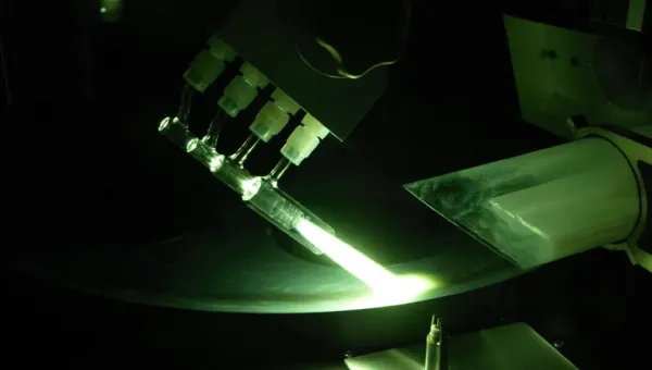
Hollow Core Fibre
Human Genetics and Genomic Medicine
Infection
Infrastructure Group
Institute of Developmental Sciences
Institute of Maritime Law (IML)
Integrated Photonic Devices
Interdisciplinary Musculoskeletal Health
International Centre for Ecohydraulics Research (ICER)
Language Assessment and Testing Unit (LATU)
Laser-Direct-Write (LDW) Technologies for Biomedical Applications
Law and Technology Centre
Long Term Conditions
Magnetic Resonance
Mathematical Modelling
Medicines Management
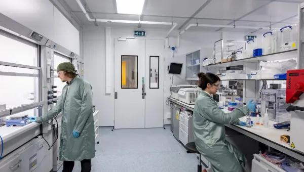
Molecular and Precision Biosciences
Multiwavelength Accretion and Astronomical Transients
National Biofilms Innovation Centre (NBIC)
National Centre for Research Methods
National Infrastructure Laboratory
Nature-Based Ocean Solutions
Nonlinear Semiconductor Photonics
Ocean Perception Group
Operational Research
Optical Engineering and Quantum Photonics Group
Paediatrics and Child Health - Clinical and Experimental Sciences
People, Property, Community
Photonic Systems, Circuits and Sensors Group
Physical Optics
Primary Care Research Centre
Quantum, Light and Matter Group
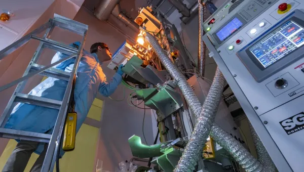
Silica Fibre Fabrication
Silicon Photonics
Skin Sensing Research Group
Southampton Ethics Centre
Southampton Health Technology Assessments Centre (SHTAC)
Southampton High Energy Physics group
Southampton Imaging
Southampton Theory Astrophysics and Gravity (STAG) Research Centre
Stefan Cross Centre for Women, Equality and Law
String theory and holography
The India Centre for Inclusive Growth and Sustainable Development
The Parkes Institute
Tony Davies High Voltage Laboratory
Ultrafast X-ray Group
Vision Science
WSA Exchange
Work Futures Research Centre (WFRC)
Support for researchers
Faculties, schools and departments
Interdisciplinary research
Find people and expertise
Research Search | Research projects
Research jobs
Business
Global